
 Search

Semiconductor.samsung.com
Samsung Electronics disclosed its first concrete performance targets for HBM5 at the Memory Executive Summit in Taipei on Tuesday, locking in a goal of roughly twice the overall capability of its current HBM4E generation — while revealing that its newly named CUBE architecture strategy covers two entirely different AI memory problems that the company's two future products are not, by Samsung's own description, solving in the same market segment. The roadmap arrived with a credibility boost that prior Samsung announcements lacked: HBM4 yield has reached 80 percent, four months ahead of the company's internal target, giving engineers a specific basis for trusting the 2028 timeline rather than treating it as aspirational.
What CUBE Actually Means — and What It Does Not Mean
The acronym stands for Capacity, Utilization, Bandwidth, and Efficiency. Samsung's VP Choi Jang-seok, head of the memory product planning team, presented the framework as a shift away from optimizing individual memory dimensions in isolation toward treating each vertical layer in a stacked die structure as a contributor to the system's overall performance per watt.
"We will no longer be constrained by the printed circuit board area," Choi said. "By expanding vertically, we can increase memory capacity without increasing the board footprint."
The enabling mechanism is through-silicon vias — copper-filled holes etched vertically through stacked silicon dies that compress the physical distance data must travel from centimeters on a circuit board to tens of micrometers within a stack. That compression is the engineering reason why structural changes in how dies are assembled translate into measurable reductions in energy per bit transmitted.
What CUBE does not mean — and this distinction the roadmap makes explicit — is that all three products under its umbrella are aimed at the same market tier. HBM5 and zHBM address server-side AI accelerators. zNAND-O addresses something else entirely.
HBM5: What the Targets Actually Are and Why 3.6 TB/s Matters More Than TFLOPS
Samsung is developing HBM5 as the successor to HBM4E, whose first 12-layer sample shipments reached major AI accelerator customers on May 29, 2026. HBM4E runs at a confirmed 3.6 terabytes per second (TB/s) of bandwidth per stack at 16 gigabits per second, in a 12-high DRAM stack configuration.
Samsung's targets for HBM5 are:
- Roughly twice the overall performance of HBM4E
- A 20 percent improvement in performance per watt
- A 20 percent reduction in thermal resistance
Applied to HBM4E's confirmed 3.6 TB/s bandwidth figure, a 2x overall performance improvement implies HBM5 operating above 7 TB/s per stack — though Samsung's "overall performance" metric encompasses capacity, efficiency, and latency in addition to raw bandwidth. The KAIST and Terabyte Interconnection and Package Laboratory roadmap cited at Hot Chips 2026 projects HBM5 entering production around 2028 at approximately 4 TB/s of bandwidth per stack per generation convention. TechTimes covered this memory wall analysis in depth.
The reason the bandwidth figure matters more than any TFLOPS specification on the AI accelerator it attaches to: large language model inference is memory-bandwidth-bound, not compute-bound. The compute silicon sits idle whenever memory cannot feed it model weights fast enough. A system that doubles TFLOPS while holding the same HBM generation delivers close to no additional inference throughput on memory-bound workloads — a structural finding Micron's HBM team quantified publicly at Hot Chips 2026.
Two engineering choices underpin HBM5's efficiency and thermal targets. Heat Path Block, first validated in HBM4E, is embedded within the die stack to function as a dedicated thermal channel — routing heat away from die-to-die interfaces, directly addressing the overheating failures that cost Samsung a generation of Nvidia supply contracts when its HBM3E chips failed qualification in 2024. HBM5's base die will be manufactured on Samsung's in-house 2-nanometer foundry process, one full node below the 4-nanometer process used for HBM4 and HBM4E. SK Hynix has built its HBM products around TSMC's 12-nanometer process for the base die — a meaningfully wider process gap than prior generations, per reporting from Seoul Economic Daily.
Volume production of HBM5 is targeted for around 2028, aimed at AI accelerator generations following Nvidia's current Vera Rubin platform.
zHBM: Eight Times HBM4E, No Production Timeline, One Unsolved Engineering Problem
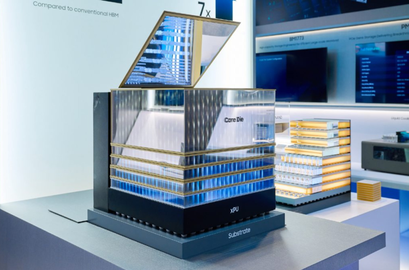
zHBM — short for zero-distance HBM — eliminates the silicon interposer that connects HBM to an AI accelerator in every current chip design by stacking HBM directly above the accelerator die, with TSV connections running vertically between the two layers. Samsung's targets for zHBM are:
- Eight times the performance of HBM4E
- Three times the performance per watt compared to HBM4E
- A 75 to 90 percent reduction in thermal resistance compared to HBM4E
Because HBM5 itself targets roughly a 2x improvement over HBM4E, zHBM's 8x target implies approximately four times the performance of HBM5 — placing it conceptually two full product generations ahead of what Samsung is actively building now. No commercial timeline has been confirmed, per Korea Herald's SEMICON Taiwan coverage.
"The key to 3D is not simply stacking components, but how each layer is utilized," Choi said. "Samsung is optimizing the placement of logic and memory to reduce data processing latency."
The engineering barrier standing between the concept and a product is thermal. An AI accelerator die generates substantial heat during inference and training; a zHBM architecture bonds that heat source directly below stacked DRAM, creating a combined thermal load more difficult to manage than the current side-by-side arrangement. Samsung presented a conceptual heat-dissipation structure that routes thermal energy laterally outward between the memory and accelerator layers, but no commercial-scale yield data supporting this approach has been made public.
The supply-chain implication of a successful zHBM architecture extends beyond performance numbers. The silicon interposer that connects HBM to AI accelerators in every current design is one of the most constrained elements in AI chip manufacturing: TSMC's CoWoS advanced packaging lines carry lead times exceeding twelve months. An architecture that eliminates the interposer requirement would restructure that bottleneck — with effects extending across every company in the AI accelerator supply chain, not only Samsung's own product portfolio.
Why Samsung's Yield Recovery Makes the Roadmap Real
AI hardware roadmaps from any memory manufacturer are targets until the fabrication line confirms otherwise. Samsung's HBM4 yield climbed from below 60 percent when mass production began in February 2026 to approximately 80 percent — the "golden yield" where volume production becomes reliably profitable — by August 2026, roughly four months ahead of the year-end target the company had set for itself, per Seoul Economic Daily reporting. HBM4E yield crossed approximately 70 percent on the same accelerated schedule, according to Sammy Fans' coverage of the milestone.
The key factor Samsung executives credit is a "turnkey" integration: the memory, foundry, and advanced packaging divisions operated as a single engineering unit from the design stage rather than as sequential handoffs. The structural advantage this creates relative to SK Hynix — which depends on TSMC for its HBM base die process — is that Samsung can optimize thermal behavior, power delivery, and interconnect characteristics simultaneously across the stack, rather than adapting to a third-party logic process, according to Seoul Economic Daily's yield analysis.
Nvidia CEO Jensen Huang confirmed in Seoul on June 5, 2026 that Samsung, SK Hynix, and Micron had all completed HBM4 qualification for the Vera Rubin platform, and that all three were in production. Current supply allocation for Vera Rubin favors SK Hynix at an estimated 60 to 70 percent of HBM4 volume, with Samsung at approximately 25 to 30 percent, according to industry analysts — reflecting SK Hynix's earlier qualification entry and its established supply relationship with Nvidia. UBS projects Samsung narrowly overtaking SK Hynix's HBM bit-shipment volume in 2027 with 41 percent share against SK Hynix's 39 percent, per BigGo Finance's analyst forecast coverage.
zNAND-O and HBF Are Not Fighting the Same Battle
This is the distinction the draft article's framing missed, and Samsung has been explicit about it: zNAND-O is not a server AI storage product.
Samsung's statement, disclosed at the FMS 2026 conference in Santa Clara in early August: "The motivation for HBF is to cover a new memory semantic tiering located right next to accelerators like GPUs in server applications, whereas zNAND-O is designed to contain large-size models to interact with the NPU in on-device applications," according to Mark LaPedus's FMS 2026 analysis.
SK Hynix's High Bandwidth Flash (HBF), developed jointly with SanDisk and standardized through the Open Compute Project at FMS 2026, targets the server memory tier between HBM and NVMe SSDs for GPU workloads — filling the gap where model weights and KV-cache data exceed HBM capacity but must be accessed faster than a standard SSD can deliver. Google and Tenstorrent are members of the HBF consortium backing it.
zNAND-O answers a different question: when a smartphone's on-device AI model — stored on NAND flash — exceeds the device's LPDDR DRAM capacity, conventional NAND flash (typically reaching sequential read speeds of 7 to 14 gigabytes per second) is too slow to load model weights into the NPU's working memory quickly enough for real-time inference. zNAND-O addresses that gap by stacking four or eight V-NAND dies using TSVs and targeting bandwidths of 200 to 400 gigabytes per second, scalable to more than 1 terabyte per second with 3D stacking, at latencies below 3 microseconds — far faster than any conventional NAND solution, per HPCwire's FMS 2026 coverage.
Samsung's published targets for zNAND-O against the relevant reference products:
- Ten times the bit density of DRAM
- Seven times the read bandwidth and power efficiency of conventional NAND storage
Customer sampling is targeted to begin in 2028.
The practical implication: Samsung and SK Hynix are solving different versions of the AI memory shortage. SK Hynix's HBF addresses the gap between GPU HBM capacity and server NVMe SSDs. Samsung's zNAND-O addresses the gap between smartphone NPU LPDDR capacity and device NAND storage. These are complementary problems in two different deployment tiers — one in the datacenter, one in the pocket.
Samsung's Market Position Heading Into the HBM5 Generation
Samsung entered the SEMICON Taiwan summit as the overall DRAM revenue leader. Counterpoint Research placed Samsung's DRAM share at 39 percent in Q2 2026, its highest since 2024, ahead of SK Hynix at 26 percent and Micron at 25 percent. TrendForce placed Samsung first in NAND revenue with 29.3 percent market share for the same period.
In HBM specifically, the gap remains. SK Hynix's own Securities and Exchange Commission filing from its 2026 US listing cited 56.4 percent global HBM market share by revenue in Q1 2026. SK Hynix CEO Kwak Noh-jung has projected that AI-driven memory shortages could persist through the end of 2030, providing a multi-year demand environment against which Samsung's CUBE roadmap will play out.
Every performance figure disclosed in Taipei represents Samsung's internal development targets, not independently audited measurements. HBM5 remains in pre-production; no customer qualification data is public.
Frequently Asked Questions
What is Samsung's CUBE strategy, and how does it relate to the products it announced?
CUBE stands for Capacity, Utilization, Bandwidth, and Efficiency. It is Samsung's stated governing framework for 3D vertical integration — the principle that every layer in a stacked semiconductor structure should be explicitly designed to contribute to the system's performance per watt, rather than optimizing individual components in isolation. The three products under the CUBE umbrella — HBM5, zHBM, and zNAND-O — target three distinct parts of the AI memory ecosystem: HBM5 for AI server accelerators through roughly 2028, zHBM as a longer-horizon post-HBM5 concept for even faster AI accelerator memory with no confirmed timeline, and zNAND-O for on-device edge AI inference via NPU acceleration. All three rely on through-silicon via technology, but they serve different deployment tiers and, in the case of zNAND-O, different customers from HBM5 and zHBM. For more on Samsung's CUBE framework and its FMS 2026 context, see Samsung's 3D Memory Architecture overview.
How much faster will HBM5 be than the HBM4E in AI systems shipping today?
Samsung's targets place HBM5 at roughly twice the overall performance of HBM4E, with a 20 percent improvement in performance per watt and a 20 percent reduction in thermal resistance. HBM4E's confirmed bandwidth at sampling is 3.6 TB/s per stack; a 2x overall performance improvement implies HBM5 will exceed 7 TB/s on a like-for-like basis, though Samsung's "overall performance" includes efficiency and capacity gains alongside raw bandwidth. Independent projections from the KAIST and Tera roadmap, cited at Hot Chips 2026, estimate HBM5 at approximately 4 TB/s per stack at production launch around 2028-2029 — the two figures are compatible if Samsung's 2x claim reflects system-level performance across all dimensions rather than single-stack peak bandwidth alone. Volume production is targeted for around 2028, per Korea Herald's SEMICON Taiwan reporting.
Is zNAND-O competing with SK Hynix's High Bandwidth Flash?
No — and Samsung has said so explicitly. SK Hynix's HBF, co-developed with SanDisk and standardized through the Open Compute Project, targets the server memory tier between GPU HBM and NVMe SSDs for large-scale datacenter AI inference. Samsung's zNAND-O is designed for on-device AI applications: storing large language model weights on a smartphone or edge device and feeding them to an NPU (neural processing unit), not to a GPU. Samsung's own language at FMS 2026 drew the distinction directly: "the motivation for HBF is to cover a new memory semantic tiering located right next to accelerators like GPUs in server applications, whereas zNAND-O is designed to contain large-size models to interact with the NPU in on-device applications." The two products solve different versions of the AI memory problem in different deployment environments, as Mark LaPedus analyzed at FMS.
Will Samsung's AI memory supercycle affect the price of PC and smartphone DRAM?
Yes — it already has. Samsung's long-term supply agreements with AI datacenter operators are expected to reserve 60 to 70 percent of its memory production for those customers, leaving 30 to 40 percent for all other buyers: smartphone manufacturers, PC makers, and enterprise storage buyers. That supply compression drove DDR5 DRAM contract prices up 90 to 95 percent quarter-over-quarter in Q1 2026, according to TrendForce. Samsung's own Galaxy smartphone division posted an operating loss in Q2 2026 partly because elevated memory component costs — driven by the same AI demand that made the semiconductor division record-profitable — could not be passed through to device buyers. The effect is structural and unlikely to reverse as long as AI datacenter buildout continues on its current trajectory, which SK Hynix's CEO has projected could persist through 2030. For the full supply-chain analysis, see Samsung zHBM supply consequences.

-
 C114 Communication Network
 -
 Communication Home
