
 Search

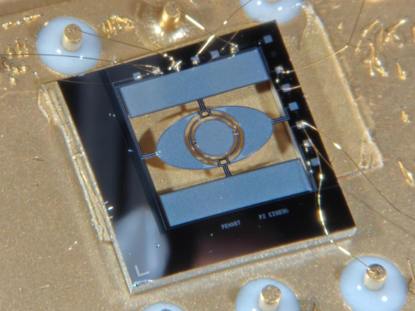
This MEMS micromirror, shown mounted and connected for testing, can steer a laser beam in two directions while also changing the mirror’s shape to refocus light at different depths. The device could help enable smaller, faster optical systems for applications including brain imaging, augmented reality and precision manufacturing. Hunter Shillingburg/Psu.edu
Getting a laser beam to do useful work in three dimensions has always demanded two separate components: one to sweep light side to side and another to pull it into focus at changing depths. Penn State University researchers have collapsed both functions into a single mirror the thickness of a penny — and it switches focus in millionths of a second, a speed that transforms what's possible in brain imaging, augmented reality, and precision manufacturing.
The device is a MEMS micromirror built on a chip roughly 1 mm (about 0.04 inches) across, built from thin films of aluminum nitride (AlN) — a piezoelectric material that flexes when voltage is applied. In a live demonstration, the team shifted the focus of a laser-scanned pattern by 63 mm (about 2.5 inches) and snapped it back to sharpness at the new depth without touching any other optical element. The work was published in Microsystems & Nanoengineering, a Nature Publishing Group journal.
"Being able to quickly control light in three dimensions with a single device offers a significant improvement in the overall size and weight of an optical system," said Hunter Shillingburg, a doctoral student in electrical engineering at Penn State and the paper's first author.
How Existing Solutions Fall Short
Three-dimensional laser control is not a new goal. Spatial light modulators (SLMs) — liquid-crystal arrays that reshape wavefronts pixel by pixel — can achieve fine beam shaping, but they are slow, power-hungry, and bulky. Liquid-crystal SLMs refresh at millisecond timescales, limited by molecular viscosity, while consuming more than 10 watts at modest resolutions. Combining a conventional two-axis scanning mirror with a separate tunable lens adds both bulk and latency, since the two components must be synchronized precisely.
The prior generation of varifocal MEMS mirrors used electrothermal actuators — structures that expand when heated by electrical current. Those devices achieved useful axial displacement but were fundamentally limited by thermal physics: heat must dissipate through the mirror substrate before the next movement can begin, restricting operation below 100 Hz. That is too slow for rapidly firing neurons, too slow for smooth AR depth transitions, and too slow for real-time surface-following in laser micromachining.
Piezoelectric actuators — which respond to voltage changes rather than temperature changes — sidestep the heat-dissipation bottleneck entirely. The Penn State device applies this insight to combine biaxial steering with varifocal tuning in a single chip-scale package, a combination that has eluded researchers working in a fabrication flow compatible with standard semiconductor manufacturing.
What's Inside: The Aluminum Nitride Piezoelectric Engine
The device uses two distinct actuation zones in the same chip. Surrounding actuators tilt the central mirror plate along two orthogonal axes — X and Y — for lateral beam steering. A separate piezoelectric layer bonded directly to the mirror plate applies curvature changes, making the reflective surface flatter or more bowl-shaped to shift where the beam converges in depth. Control both simultaneously and you have complete, real-time, three-dimensional command over a laser beam in a package no larger than a fingernail clipping.
The actuating material, aluminum nitride (AlN), is the device's architectural centerpiece. Unlike lead zirconate titanate (PZT) — the piezoelectric workhorse of the prior generation — AlN deposits below 400°C, enabling CMOS integration and contains no lead. PZT requires between 500°C and 700°C (932°F to 1,292°F) for deposition, and its lead content risks contaminating the shared tooling that semiconductor fabs use for logic transistors. That contamination concern is not cosmetic: it has historically meant building AlN on entirely separate process lines, which drives up cost and complexity. AlN sidesteps both problems.
That CMOS compatibility is not merely a manufacturing convenience — it is the enabling architectural decision that makes the entire miniaturization promise real. Without it, the mirror still requires external control boards and off-chip wiring that largely offset the size and weight advantages the device provides. With it, the mirror can eventually be co-integrated with its drive electronics on a single chip, cutting wiring complexity, reducing latency, and opening a path to true system-on-chip 3D optical control.
The tradeoff is one engineers know well: AlN produces weaker piezoelectric response than PZT, which limits the actuation range achievable at a given voltage. The Penn State team plans to address this through refined fabrication tolerances, and current research across the field is exploring scandium-doped AlN (AlScN) as a way to boost the coefficient without surrendering CMOS compatibility.
Because the mirror is only about 1 mm (0.04 inches) across, its mechanical resonant frequency is high — and that high frequency is why the mirror responds in microseconds rather than milliseconds. Larger mirrors ring at lower frequencies; this one rings fast enough to shift focus before a neuron has finished firing. The researchers measured focus transitions within millionths of a second, a speed relevant to quantum control experiments, structured illumination microscopy, and optogenetics for neuron control — the technique that uses light to monitor and selectively activate individual neurons.
What Is a MEMS Micromirror?
MEMS — micro-electromechanical systems — are miniaturized machines built on semiconductor chips using the same photolithography and deposition techniques that produce computer chips. Components range from roughly 1 micrometer to a few millimeters in size and can include mechanical structures — springs, levers, and mirrors — alongside electronic circuits. MEMS accelerometers sense G-forces inside smartphones; MEMS gyroscopes tell drones which way is up; MEMS micromirrors drive the image chips inside laser projectors and digital cinema cameras.
A MEMS micromirror is, at its simplest, a mirror that can tilt. "A MEMS micromirror is simply a mirror that can move," Shillingburg explained. "Like a regular mirror, shining a laser at it causes the beam to reflect off the mirror's surface, and the reflected beam spot can be positioned by tilting the mirror back and forth." What the Penn State device adds to that basic picture is curvature control — the mirror's surface changes shape, not just angle, which means it acts as both a steering mirror and a dynamic lens at once.
Three Fields That Stand to Benefit
Brain imaging and neuroscience. Neurons fire on timescales of milliseconds. Capturing the cascade of activity across even a small patch of cortex demands a light-delivery system that can hop between hundreds of points — at varying depths in a scattering tissue — faster than the biology itself. Current MEMS-based miniature two-photon microscopes have achieved head-mounted designs weighing 2.15 grams that can ride on a freely moving mouse, but combining lateral scanning and depth control in a single component has remained a fabrication challenge.
"Although the fields are all strongly related, I see the most potential being in neurobiology," Shillingburg said. "The system could lead to smaller mountable miniature microscopes for studying neurobiology in active subjects as well as lighter glasses and headsets for augmented reality." Faster scanning also reduces the light dose each cell receives — a meaningful benefit when imaging living tissue, since prolonged laser exposure can bleach fluorescent labels or damage cells outright.
Augmented reality displays. Every major AR headset on the market today projects virtual content at a fixed focal distance — the distance from the display panel to the optics. When the virtual scene depicts an object that appears to be close, the viewer's eyes converge on that virtual object at one apparent depth while the display forces them to focus at another. That mismatch, called the vergence-accommodation conflict, is an established source of eye strain, visual fatigue, and headaches during extended AR use. A 2024 study in augmented reality confirmed that the time a user needs to refocus between a real-world object and an AR overlay increases exponentially as the vergence-accommodation mismatch grows.
"Fixed focus displays can lead to eye strain largely because the object is generated on a panel," Shillingburg noted. "Many of these devices have adjustable screen distances to better accommodate users with different vision needs, and although this helps to alleviate the eye strain, it doesn't get rid of it." A scanned display built around a mirror that actively shifts its focal plane could make virtual objects at different simulated distances feel more natural to the visual system, potentially unlocking longer and more comfortable AR sessions.
Precision laser micromachining. High-value manufacturing increasingly relies on tightly focused lasers to cut, ablate, or texture surfaces at micron-scale resolution. If the workpiece surface undulates — as cast or machined metal parts typically do — the laser drifts out of focus, introducing defects. A micromirror that adjusts laser focus in real time on the fly could measurably improve yield in the fabrication of precision components.
Known Limitations and What Comes Next
The Penn State team is transparent about the device's current imperfections. Slight asymmetry in the mirror geometry introduces aberrations in the reflected wavefront — the beam is slightly distorted at the edges of its scan range. The researchers plan to address this through refined fabrication tolerances and post-fabrication calibration. Further performance improvements are also on the roadmap for applications demanding even faster scanning, such as multiphoton microscopy or free-space optical communications.
Co-authored by Shillingburg and Daniel Lopez — who was affiliated with Penn State's Department of Electrical Engineering and Computer Science and Materials Research Institute at the time of the research and is now chair of the Department of Physics at Arizona State University — the work was published in Microsystems & Nanoengineering, a Nature Publishing Group journal.
The 63 mm (about 2.5-inch) focal shift and microsecond switching speed represent a landmark in what a single semiconductor-compatible chip can achieve in three-dimensional optical control. The question now is how quickly the fabrication community can adopt the process and whether AlScN — with its enhanced piezoelectric output — can push the scan range further without sacrificing the CMOS compatibility that makes the device manufacturable in the first place.
Frequently Asked Questions
What is a MEMS micromirror, and what makes this one different from conventional ones?
A MEMS micromirror is a small mirror — typically a fraction of a millimeter to a few millimeters across — fabricated on a semiconductor chip using the same techniques used to build computer processors. Conventional MEMS scanning mirrors can tilt in one or two axes to steer a laser beam laterally. The Penn State device adds a third capability: it also changes the curvature of its own reflective surface, which shifts where the laser beam comes into focus in depth. That combination of lateral steering and focal tuning in a single chip-scale device — operating at microsecond speeds and built with CMOS-compatible aluminum nitride — is what distinguishes it from prior designs. Background on MEMS technology is available from Encyclopaedia Britannica's MEMS overview.
Why does it matter that the mirror uses aluminum nitride instead of the more common PZT?
Lead zirconate titanate (PZT), the dominant piezoelectric material in previous MEMS mirror research, requires deposition temperatures of 500°C to 700°C (932°F to 1,292°F) and contains lead, which can contaminate the shared tooling used in standard semiconductor fabs. That contamination risk has historically forced researchers to process PZT on entirely separate equipment lines — raising costs and making it difficult to co-integrate the mirror with electronics. Aluminum nitride deposits below 400°C, lead-free, making it fully compatible with standard CMOS semiconductor manufacturing. The practical consequence: a future product could potentially place the mirror and its drive circuits on the same chip, reducing size, weight, and signal latency. The tradeoff is that AlN produces a weaker piezoelectric response per volt than PZT, which limits the achievable scan range at low voltages — a constraint the field is actively working to address through scandium doping.
How does this device address the eye strain problem in AR headsets?
The core issue in today's AR headsets is a mismatch called the vergence-accommodation conflict explained here: your eyes physically point toward a virtual object at one apparent distance, but the headset's display requires your eyes to focus at a fixed optical distance — typically a meter or more away. Your visual system expects both cues to match, and when they don't, the discrepancy causes fatigue, blurring, and headaches. A micromirror that rapidly shifts the focal plane of a scanned display could allow virtual objects at different simulated depths to actually feel focused at those depths, eliminating the mismatch. The Penn State device's microsecond response time is fast enough to track gaze and update focus within a single video frame, which is the speed threshold needed to make the effect imperceptible to the viewer.
What does "CMOS-compatible" mean and why does it matter for this research?
CMOS stands for complementary metal-oxide-semiconductor — the dominant manufacturing process used to build the logic chips inside every smartphone, laptop, and server. When a material or process is described as CMOS-compatible, it means it can be introduced into a standard chip fab without contaminating the tooling or disrupting the other process steps. For this mirror, CMOS compatibility means the fabrication process could eventually run on the same production line as the drive electronics that control the mirror, allowing the two to be combined on one chip. That integration eliminates off-chip connectors, reduces wiring-induced signal delay, and dramatically shrinks the overall system size — which is essential for the head-mounted neuroscience microscopes and lightweight AR headsets the team has in mind. Full fabrication details are in the Shillingburg and Lopez paper.

-
 C114 Communication Network
 -
 Communication Home
