
 Search

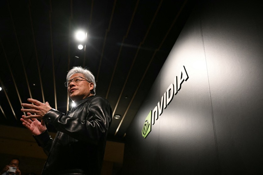
Nvidia CEO Jensen Huang attends the Q&A session with the media during Nvidia/Japan AI Ecosystem Reception in Tokyo on July 16, 2026. Philip FONG/AFP via Getty Images
NVIDIA's newest memory architecture for custom AI accelerators does something that no commercially available high-bandwidth memory standard has done before: it moves the memory controller off the processor chip entirely and buries it inside the HBM base die itself — freeing up to 25% more compute area on the accelerator for actual compute logic. That architectural inversion, announced August 26 and formalized in an expanded partnership with MediaTek announced August 31, is the technical foundation that makes MediaTek's new role as the custom XPU integration gateway for NVIDIA's ecosystem possible.
NVIDIA and MediaTek announced a deepening of their longstanding collaboration to build the next generations of AI computing platforms spanning AI infrastructure, local AI computing, and automotive. The partnership is anchored by a $3.5 billion NVIDIA convertible bond investment in MediaTek — the largest single subscriber position in MediaTek's record $3.9 billion overseas offering — and reorganizes how hyperscalers and cloud providers build custom AI chips for NVIDIA-connected rack-scale data centers. Under the agreement, MediaTek becomes the integration and manufacturing partner for custom XPUs that adopt NVIDIA's NVLink Fusion platform and new NVHBM memory architecture — giving hyperscalers a pre-validated rack-scale deployment path without independently mastering NVIDIA's proprietary interconnect specification.
NVHBM: What Moving the Memory Controller Into the HBM Stack Actually Means
In every AI accelerator built on standard HBM4e today, the memory controller on XPU die — the logic that manages all communication between the processor and its high-bandwidth memory stacks — consumes precious silicon area that could otherwise hold more matrix multiply engines, vector units, or cache hierarchy. At the density of TSMC's leading-edge nodes, every square millimeter of compute die area is worth allocating carefully.
NVHBM eliminates that tradeoff by integrating NVIDIA's custom memory controller and a proprietary physical interface (PHY) directly into the HBM base die — the foundation layer of the 3D-stacked memory package. The compute die then connects to the HBM stack through a much narrower interface than the JEDEC HBM4e standard requires. The results, according to NVIDIA's technical specification: PHY and supporting area on the XPU compute die shrinks by up to 67% compared with JEDEC HBM4e; up to 25% more of the XPU's main die becomes available for compute or other features; memory bandwidth per stack increases by up to 30% over HBM4e; and HBM power consumption falls by up to 15%. The compound effect of those improvements translates to a stated 30% end-to-end XPU performance increase.
The interposer routing simplification that follows from NVHBM's narrower memory interface is also significant: NVIDIA says the smaller interface provides up to 80% more usable silicon across the entire package layout, giving package designers more flexibility to arrange memory stacks, I/O connections, and power delivery without the routing congestion that wide HBM interfaces create.
At data center scale, the power savings compound in ways the per-chip numbers do not immediately suggest. In a one-gigawatt data center operating 2,000-watt accelerators, the 15% reduction in HBM power consumption, propagated across the entire fleet, could enable up to 15,000 additional XPUs within the same power and thermal envelope. That figure represents compute capacity added not by adding power, but by spending memory power more efficiently.
Amazon's Annapurna Labs, which designs the AWS Trainium series of custom AI training chips, is the first announced collaborating partner with NVIDIA on NVHBM alongside NVLink Fusion adoption. The integration positions AWS Trainium4 silicon to connect into the same NVLink fabric as NVIDIA GPUs, enabling rack-scale systems where both chip types coexist and communicate at NVLink bandwidth rather than PCIe speeds.
Read more: AWS Adds 2 Million More NVIDIA GPUs: Prior 1 Million Commitment Ran Out Early
MediaTek's New Role: XPU Integration Gateway for Hyperscalers
The practical obstacle that NVLink Fusion and NVHBM together address is a development bottleneck familiar to any team that has tried to deploy custom silicon in an NVIDIA-powered data center. Before NVLink Fusion, a hyperscaler that wanted to pair its own custom XPU with NVIDIA GPUs in the same rack faced a lengthy engineering program: qualify every layer of the surrounding architecture, from memory and packaging through high-speed SerDes, I/O, and scale-up networking, against NVIDIA's proprietary interconnect specifications. That qualification work consumed engineering resources independent of the actual differentiated compute the hyperscaler wanted to build.
MediaTek's expanded role under the August 31 agreement changes that equation. Hyperscalers bring their XPU designs to MediaTek. MediaTek produces chips that incorporate the NVLink Fusion chiplet — NVIDIA's pre-built, pre-validated interface that connects custom XPUs to the NVLink scale-up fabric through photonic or electrical interconnects. What the hyperscaler delivers to its data center is a chip that has already passed NVIDIA's rack-scale validation — without the hyperscaler's engineering team having to own that qualification process themselves.
"Rather than engineering and qualifying every element surrounding a custom XPU from the ground up, customers can focus resources on the differentiated compute that defines their platforms," NVIDIA and MediaTek said in their joint statement.
Three components constitute the NVLink Fusion platform that MediaTek will offer as a design foundation. The NVLink Fusion chiplet bridges the custom XPU to NVIDIA's NVLink fabric using a UCIe (Universal Chiplet Interconnect Express) bridge at the die-to-die level and NVLink protocol at the fabric level. NVLink-C2C provides chip-to-chip links at 300 gigabytes per second (GB/s) bidirectional bandwidth between XPUs, NVIDIA's Vera CPUs, and other compatible processors. And NVHBM provides the memory architecture described above.
NVIDIA's sixth-generation NVLink scale-up fabric connecting those XPUs within a rack delivers 260 terabytes per second bandwidth of aggregate bandwidth in a single 72-chip domain, with end-to-end latency that NVIDIA documents as three times lower than comparable Ethernet-based scale-up alternatives. The NVLink Switch chips and PHY layers that govern the fabric remain under NVIDIA's exclusive control — meaning every XPU in the NVLink Fusion ecosystem must connect to an NVIDIA product to access the network.
Three Partnership Pillars: Infrastructure, Local AI, and Automotive
The NVHBM-anchored infrastructure collaboration is the first of three pillars NVIDIA and MediaTek formalized on August 31.
The second is a commitment to co-develop multiple future generations of both the DGX Spark and RTX Spark chip lines. MediaTek co-designed the GB10 Grace Blackwell Superchip at the heart of the DGX Spark personal AI supercomputer, which began shipping in October 2025. The GB10 integrates a 20-core Arm Grace CPU and a Blackwell-generation GPU connected via NVLink-C2C at 300 GB/s, with 128 gigabytes of unified memory — sufficient to run inference on models up to 200 billion parameters on a desktop device that draws from a standard wall outlet. Two connected DGX Spark units, linked through onboard ConnectX-7 networking, can handle models up to 405 billion parameters.
RTX Spark, announced at Computex Taipei in June 2026, extends the Grace-plus-Blackwell architecture to Windows 11 consumer laptops and compact desktops — combining a 20-core Grace CPU (co-developed with MediaTek) and a Blackwell RTX GPU in an Arm-based system-on-chip targeting personal AI agents, creative workloads, and gaming. Six OEM partners launching fall 2026 — ASUS, Dell, HP, Lenovo, Microsoft Surface, and MSI — are expected to ship RTX Spark-based devices in fall 2026.
The third pillar is automotive. MediaTek's Dimensity Auto Cockpit Platform C-X1 — built on a 3nm process with an Arm v9.2-A CPU architecture and a Blackwell-generation RTX GPU — already integrates NVIDIA RTX graphics and can co-exist with NVIDIA's DRIVE AGX autonomous-driving platform and DriveOS software. The companies committed on August 31 to extend the collaboration across multiple future automotive silicon generations, targeting the software-defined vehicle market where cockpit intelligence and autonomous-driving compute increasingly converge on a shared hardware platform.
What NVHBM Signals About Who Controls the AI Infrastructure Stack
NVIDIA's decision to open NVLink to third-party XPUs through NVLink Fusion — while retaining exclusive control of the switch chips, PHY layers, and communication controllers — reflects a calculated architectural strategy. As hyperscalers deepen their commitment to custom silicon (AWS Trainium, Google TPUs, Microsoft Maia, Meta MTIA), NVIDIA's risk is that its GPUs become optional at the compute layer. NVLink Fusion is designed to ensure NVIDIA participates in custom AI silicon economics at the interconnect and memory layers even when a hyperscaler chooses not to buy an NVIDIA GPU as the primary compute engine.
The move to NVHBM extends that logic one layer deeper, into the memory subsystem itself. A hyperscaler XPU that adopts NVHBM now sources its memory architecture from NVIDIA, connects to the NVLink fabric through NVIDIA's chiplet, and operates in racks running NVIDIA's switch infrastructure. NVIDIA's involvement in the data center economics is present whether or not the compute die carries the NVIDIA brand.
Matt Kimball, vice president and principal analyst at Moor Insights and Strategy, framed the broader dynamic: "Heterogeneity is the future of AI." As inference workloads proliferate and hyperscalers mature their custom silicon programs, AI infrastructure becomes a more complex mix of GPUs and specialized accelerators — all of which need to communicate quickly inside large systems. NVIDIA's network and memory architecture, wrapped around third-party compute, is designed to remain indispensable in that heterogeneous world.
For MediaTek, the role of XPU integration gateway opens a market that is structurally different from its mobile SoC business. Serving hundreds of hyperscaler and frontier AI model developers building custom accelerators requires the ASIC design services, advanced packaging relationships, and high-speed interface expertise that MediaTek has built over decades in high-volume consumer silicon. The $3.5 billion investment from NVIDIA — a convertible bond that gives NVIDIA equity upside if MediaTek's AI chip business grows — signals that both companies expect that addressable market to be large enough to warrant structural financial alignment.
Read more: Nvidia Bets $3.5B on MediaTek Convertible Bonds, Fueling Circular Financing Debate
Competing Interconnect: UALink 2.0 Arrives in April 2026
NVHBM and the MediaTek XPU factory partnership land as the open-standard alternative to NVLink enters its second major revision. The UALink Consortium — whose members include AMD, Intel, Google, Microsoft, Meta, Apple, AWS, HPE, and Cisco, but not NVIDIA — published the UALink 2.0 specification in April 2026, updating the open scale-up interconnect standard it first ratified in April 2025. UALink is designed to enable the same scale-up connectivity that NVLink provides, but on an open specification that multiple hardware vendors can implement — meaning hyperscalers building on UALink are not structurally dependent on NVIDIA switching silicon.
Commercial switch products supporting UALink were not yet available at production scale as of September 2026, giving NVIDIA a window during which NVLink Fusion is the only production-ready option for hyperscalers that want to connect custom XPUs to a proven rack-scale AI fabric. Whether that window closes before UALink switching reaches production scale will significantly influence how many XPU programs commit to NVLink Fusion's interconnect dependency for their next silicon generation.
What the NVHBM Figures Actually Represent Right Now
One technical caveat deserves specific attention for any engineering team using these figures in procurement decisions: every NVHBM performance specification — the 30% bandwidth improvement, the 25% more compute die area, the 15% lower power consumption, the 30% end-to-end XPU performance gain — is an architectural specification from NVIDIA, not a measurement taken from a shipping product. As of September 2026, no independent benchmark organization has published measurements of a physical NVHBM-equipped accelerator.
That is not a red flag on its own. NVIDIA's track record of delivering on stated architectural specifications is strong, and the underlying mechanisms — moving the memory controller to reduce PHY area, using narrower interface connections — are grounded in established semiconductor physics. AWS Annapurna Labs' early collaboration on NVHBM for Trainium4 provides an independent signal from Annapurna Labs that at least one major customer has evaluated the architecture and found it credible. But procurement teams should treat NVHBM-derived performance projections as pre-production architectural targets until independently verified on shipping silicon — a distinction that matters when planning AI data center capacity.
Frequently Asked Questions
What does "moving the HBM memory controller to the base die" actually mean for a custom AI chip?
In a standard HBM configuration (the current JEDEC HBM4e specification), the logic that manages communication between the processor and its memory stacks sits on the processor die itself. This memory controller consumes silicon area that could otherwise hold more compute units — matrix multiply engines, vector processors, or cache. NVHBM integrates NVIDIA's custom memory controller directly into the HBM base die (the foundation layer of the 3D memory stack), along with a custom physical interface. The processor die then connects to memory through a narrower interface. The result is that up to 25% more of the XPU compute die becomes available for compute logic — without adding more chips or expanding the package footprint. For hyperscalers building workload-specific XPUs where every square millimeter of compute area matters, that freed silicon can mean more inference throughput, more specialized processing units, or more SRAM within the same cost and packaging constraints.
If MediaTek now handles XPU integration for hyperscalers, what does that change for how quickly a cloud company can deploy custom silicon?
Previously, a hyperscaler that wanted to connect its custom XPU to an NVIDIA-powered rack had to independently qualify its chip against NVIDIA's proprietary NVLink interconnect specification — a hardware and software validation program that adds engineering time and resource cost on top of the XPU design itself. Under the MediaTek NVLink Fusion integration model, MediaTek handles that qualification as part of producing the chip. The XPU arrives pre-validated for NVIDIA rack-scale deployment via the embedded NVLink Fusion chiplet. The hyperscaler still owns the compute die design — the differentiated silicon. MediaTek owns the surrounding integration complexity. This shortens the path from "custom XPU silicon tape-out" to "deployed in a production AI factory," which is meaningful when hyperscalers are competing to bring inference capacity online faster.
Does adopting NVLink Fusion and NVHBM lock a hyperscaler into NVIDIA infrastructure permanently?
Structurally, yes — at the interconnect layer. NVIDIA retains exclusive control of the NVLink Switch chips, the PHY layers, and the communication controllers that govern the NVLink fabric. A custom XPU built around the NVLink Fusion chiplet cannot operate in a fabric that doesn't include NVIDIA switching infrastructure. The open alternative — UALink, published by a consortium that includes AMD, Intel, Google, Microsoft, Meta, and AWS — reached version 2.0 in April 2026, but commercial switch products were not yet at production scale as of early September 2026. Hyperscalers that commit to NVLink Fusion for their next XPU generation are betting that the integration advantages and performance credentials of NVIDIA's fabric outweigh the structural dependency — or that they can run parallel XPU programs on different interconnect standards. Some, like AWS, appear to be pursuing both paths simultaneously.
When will NVHBM-equipped chips actually ship?
NVIDIA has not announced a specific shipping date for NVHBM-equipped XPUs beyond indicating that Amazon's Annapurna Labs is the first announced customer collaborating on Trainium4 integration. NVHBM is a pre-production architecture as of September 2026; no independently benchmarked silicon has been published. The MediaTek NVLink Fusion design services path — through which hyperscalers bring XPU designs and receive chips with the NVLink Fusion chiplet — is currently available, but NVHBM-enabled designs will follow the normal silicon development and qualification timeline from the time hyperscalers begin their tape-outs.

-
 C114 Communication Network
 -
 Communication Home
