
 Search

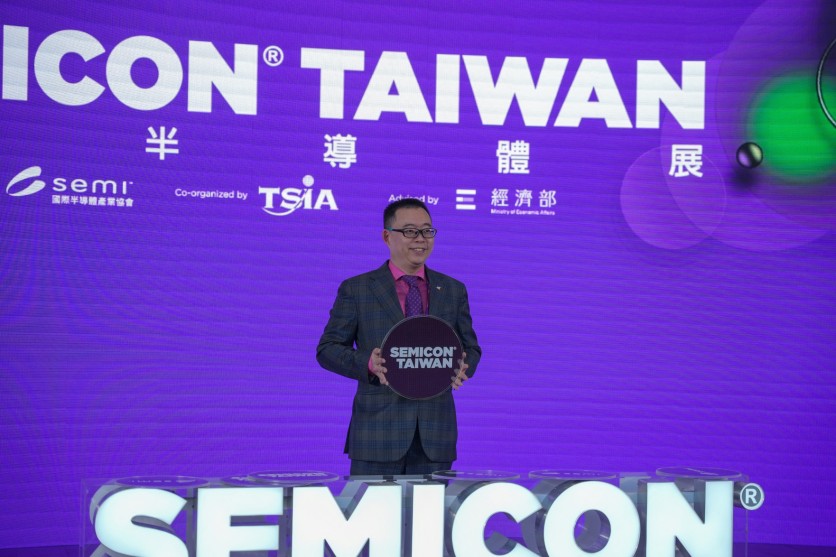
A man holds a prop wafer with Semicon Taiwan logo printed on it at the Semicon Taiwan 2024 in Taipei on September 4, 2024. WALID BERRAZEG/gettyimages.com
The semiconductor industry's most authoritative annual gathering launched its forum program Monday morning in Taipei, as SEMICON Taiwan 2026 opened International Semiconductor Week — and the central engineering question driving nearly every session is no longer which chip is fastest. It is whether the wires connecting chips can keep up at all. SEMI's August 2026 official announcement confirmed the event's record scale and dates.
"Data movement in today's AI systems could consume more energy than computation itself, making system architecture, not individual chip performance, the new bottleneck," said Terry Tsao, Global Chief Marketing Officer and President of Taiwan at SEMI, the industry association that organizes the event. That single sentence maps the entire SEMICON Taiwan 2026 agenda: silicon photonics, high-bandwidth memory, heterogeneous integration, and advanced packaging are not parallel industry concerns but engineering responses to the same constraint — the widening gap between how fast chips compute and how fast data can physically move between them. The EDN Asia SEMICON Taiwan preview reports that frontier AI training compute is growing four- to fivefold annually, pushing power and data movement to the center of the performance race alongside raw compute.
The IC Forum, Silicon Photonics Global Summit, and MEMS & Sensors Forum opened Monday at Grand Hilai Taipei, with the Fan-Out Panel Level Packaging (FOPLP) Innovation Forum and the imec Technology Forum Taiwan following in the afternoon. The official SEMICON Taiwan 2026 forum schedule confirms sessions across five days through Friday, September 4, with the program hosting more than 22 forums, summits, and partner events before the three-day main exhibition opens at the Taipei Nangang Exhibition Center (TaiNEX) Halls 1 and 2 on Wednesday, September 2.
The 2026 edition is record-setting across every measurable dimension: more than 1,300 exhibitors, 4,300 booths, 18 national pavilions, and more than 100,000 professionals expected from 65 countries — all figures surpassing any prior year. Global semiconductor manufacturing equipment sales reached $135.1 billion, up 15% year-over-year, per SEMI data cited at the event. SEMI's April 2026 300mm Fab Outlook separately projects 300mm fab equipment spending will reach $133 billion in 2026 and $151 billion in 2027 — the first time the industry will have ever crossed the $150 billion threshold in a single year. The forecast extends through 2029, with spending projected at $155 billion in 2028 and $172 billion in 2029. SEMI CEO Ajit Manocha has described this as "AI resetting the scale of semiconductor manufacturing investment" in response to surging demand for advanced-node AI chip capacity and semiconductor self-sufficiency efforts across multiple regions.
Why Copper Wires Are Losing the AI Race
The forum structure of SEMICON Taiwan 2026 is not arbitrary. It maps directly onto an engineering crisis that SEMI and its member companies consider more acute than any chip design challenge.
AI clusters today require data movement between thousands of GPUs, switches, and memory systems at rates exceeding 100 terabits per second per node. Copper interconnects — the standard technology for on-board and between-board chip communication — are reaching their physical limits. Electrical signaling over copper requires equalization and retiming circuits that consume power proportional to the data rate; at AI-cluster speeds, those overheads become dominant. Signal integrity degrades with distance, and thermal dissipation grows faster than the performance gains from adding more compute.
Co-packaged optics (CPO) is the leading engineering response. CPO integrates optical engines — photonic components that transmit data using light rather than electrons — directly within the switch ASIC package, reducing the signal path from centimeters (copper traces on a board) to millimeters (optical connections in a package). The result is bandwidth density and power efficiency that copper cannot match at AI scale. The EDN Asia CPO 2026 overview details how Taiwan's supply chain is converging on this architecture.
This year at SEMICON Taiwan, CPO moved from a technology roadmap slide to a production question. Taiwan Semiconductor Manufacturing Co.'s (TSMC's) Compact Universal Photonic Engine (COUPE) platform entered mass production in 2026. The SiPhIA forum COUPE mass production milestone confirmed three key breakthrough areas: wafer testing, fiber array units, and high-speed optical packaging assembly. United Microelectronics Corp. (UMC) completed its first mass-produced silicon photonics wafers at its Singapore fab in partnership with Silith Technology. GlobalWafers entered volume production for some silicon photonics products earlier this year. Hon Hai Precision Industry (Foxconn) expects to begin CPO switch shipments in the third quarter of 2026. Hon Hai affiliate ShunSin Technology, through a TSMC collaboration, has achieved mass production capability for 51.2-terabit (Tbps) and 102.4 Tbps CPO products. Powertech Technology, partnering with Broadcom, plans low-volume production for optical engine components in 2026 before integrating them into full CPO switches in 2027. The Taipei Times CPO commercialization report provides detailed coverage of each company's production milestone.
The breakthrough areas that determine whether CPO scales to volume, per TSMC's own assessment at a Silicon Photonics Industry Alliance forum in April 2026: wafer testing, fiber array units, and high-speed optical packaging assembly. Those are exactly the challenges the Silicon Photonics Global Summit addressed when it opened Monday morning.
Read more: TSMC Revives Longtan for 1.4nm Fabs and CoWoS Hub as Both Sell Out Globally
Monday, August 31 — Forum Opening Day
IC Forum: Advanced Chip Technology and Manufacturing
8:30 am – 4:55 pm | Platinum Ballroom C, Grand Hilai Taipei
The IC Forum opened Monday morning under the theme Synergetic Advanced Nodes: Empowering AI for Chips & Crafting Next-Gen AI Silicon. The SEMICON Taiwan official forum program confirms the full day's agenda. The forum, chaired by Dr. John Lin of TSMC's Lithography R&D division, maps the transition from FinFET architectures through Gate-All-Around (GAA) nanosheet devices and into Backside Power Delivery Network (BSPDN) architectures — each step driven by the need to reduce power consumption and improve logic density for AI workloads. The enabling technologies reviewed span Extreme Ultraviolet (EUV) lithography, Atomic Layer Deposition (ALD), and AI-native Electronic Design Automation (EDA) tools.
The morning opened with TSMC's April Li presenting on leadership silicon and system integration, followed by sessions from Merck (AI-driven materials innovation velocity), imec's Dr. Philippe Leray (High-NA EUV lithography), and Lam Research's Dr. Gowri Kamarthy (plasma etch technologies for 3D AI device structures). Applied Materials, Tokyo Electron, ASML, ZEISS SMT, ASM, and Siemens EDA each address their respective roles in enabling the next-generation process node.
Monday IC Forum afternoon sessions include:
| Time (Taipei) | Session | Presenter |
|---|---|---|
1:35 pm | High-NA EUV for High-Volume Manufacturing | Greet Storms, ASML |
2:00 pm | Optics for Advanced Chip Manufacturing | Dr. Heiko Feldmann, ZEISS SMT |
2:25 pm | ALD Innovations for Advanced Nodes | Dr. Abhudaya Mishra, ASM |
2:50 pm | Advanced CMP Pad Engineering for AI Chip Planarization | Dr. Ivan Li, Qnity Electronics |
3:30 pm | Patterning Landscape in AI-Driven Manufacturing | Dr. Douglas Guerrero, Brewer Science |
3:55 pm | AI-Native EDA: Designing Chips That Power the Future | Sathish Balasubramanian, Siemens |
4:20 pm | Advanced Nodes, Next-Generation Silicon, Supply Chain | Helen Chiang, IDC |
Silicon Photonics Global Summit
8:30 am – 5:05 pm | Platinum Ballroom B, Grand Hilai Taipei
The first standalone Silicon Photonics Global Summit in SEMICON Taiwan's history opened Monday as SEMI's designated flagship event for the interconnect transition. SEMI's Silicon Photonics Global Summit announcement explains the summit's co-equal status with the IC Forum. The summit is co-chaired by K.C. Hsu, VP of Advanced Packaging Technology Development at TSMC, and Dr. C.P. Hung, VP of Corporate R&D at ASE Inc., and is advised by the SEMI Silicon Photonics Industry Alliance.
The session lineup runs from system architecture to wafer-level testing: Cisco opened on AI connectivity scaling for next-generation infrastructure; TSMC's Ming Fa Chen presented on COUPE, the company's co-packaged photonic engine platform; Lumentum, Marvell, UMC, Lightmatter, ASE, imec, Soitec, Lam Research, Onto Innovation, ficonTEC, Advantest, and ENLI Technology each addressed a specific layer of the silicon photonics manufacturing and deployment stack.
Also exhibiting at SEMICON Taiwan 2026: AUO Group's Daxin Materials subsidiary, which is showcasing a system-level Micro LED CPO module designed for short-reach AI data center interconnects of up to 10 meters (32.8 ft), integrating transmitters from Ennostar and photodetector receivers from Tyntek. The AUO GlobeNewswire August 31 announcement describes the full system-level module design.
MEMS & Sensors Forum
8:15 am – 4:35 pm
Running concurrently with the IC Forum Monday, the MEMS & Sensors Forum addresses the micro-electro-mechanical systems and sensor technologies serving automotive, industrial IoT, and consumer electronics markets — a segment growing in strategic importance as automotive chips and edge AI devices increasingly rely on heterogeneous sensor integration.
FOPLP Innovation Forum (HIGS Series Event)
1:00 pm – 5:00 pm
Fan-Out Panel Level Packaging (FOPLP) is emerging as a cost-effective alternative to wafer-level packaging for AI chip assembly. Unlike wafer-level approaches, FOPLP processes chips on large rectangular panels, potentially enabling lower-cost high-throughput packaging for the chiplet architectures that AI accelerators increasingly use. This afternoon session is part of the Heterogeneous Integration Global Summit (HIGS) series.
Partner Program: ITF Taiwan — imec Technology Forum
1:00 pm – 5:30 pm
imec's Technology Forum Taiwan brings the Belgian research hub's perspective on logic scaling, memory, and advanced packaging to Taipei's industry audience. imec's researchers are directly involved in High-NA EUV lithography development and advanced packaging roadmap planning — making ITF Taiwan a key venue for understanding where process technology is heading over the next three to five years.
Tuesday, September 1
Heterogeneous Integration Global Summit (HIGS) — Day 1
8:30 am – 4:30 pm
Heterogeneous integration — the discipline of assembling chips designed on different process nodes into a single package — is the architectural foundation that makes AI accelerators economically possible. Rather than requiring all functions on one monolithic die (which would demand the most expensive available process node for every circuit), HI allows designers to use advanced nodes only where they deliver the most value, and pair them with optimized dies for memory, I/O, or photonics. Day 1 of HIGS will cover advanced packaging architectures, chiplet ecosystems, and the substrate technologies enabling these multi-die systems.
Power and Compound Semiconductor Forum | NExT Forum
8:30 am – 4:50 pm
Compound semiconductors — gallium nitride (GaN), silicon carbide (SiC), and indium phosphide (InP) — are central to the power electronics enabling electric vehicle charging infrastructure, renewable energy inverters, and the RF communications systems underlying 5G and emerging 6G deployments. The NExT segment addresses emerging device architectures for the next decade's power applications.
Partner Program: Quantum Taiwan Forum — Full Stack
8:30 am – 5:10 pm
Taiwan is making a substantial push into quantum computing infrastructure. This full-day forum covers the complete quantum stack: qubit fabrication methods (including silicon spin-qubit approaches using standard CMOS processes), cryogenic electronics, quantum error correction, and system integration — with participation from both academic research institutions and commercial quantum computing companies.
Market and Industry Trend Forum
8:40 am – 12:00 pm
This morning session delivers macroeconomic and strategic analysis for the global semiconductor sector. Global semiconductor revenues are expected to approach $975 billion by 2026, with the memory segment projected to exceed $440 billion. The forum provides the strategic context in which every technology decision discussed throughout the week is being made.
Smart Manufacturing Forum
8:40 am – 4:45 pm
AI-driven manufacturing is transforming fab operations from predictive maintenance and yield optimization to autonomous process control. This full-day forum covers AI-native factory operations, digital twin technology, and the tools enabling next-generation fab intelligence — an increasingly critical discipline as chip architectures grow more complex and the cost of defects at advanced nodes rises.
GES Taiwan 2026 Executive Summit on Energy and Sustainability
7:45 am – 7:00 pm (Full Day) | 1:30 pm – 7:00 pm (Afternoon Session)
Energy consumption has become one of the chip industry's most acute strategic challenges. The EDN Asia AI power constraints report notes that frontier AI training compute is growing four- to fivefold annually. The GES Taiwan Summit addresses how the semiconductor industry can meet net-zero commitments while scaling AI infrastructure, with sessions spanning fab energy efficiency, renewable sourcing, and water management. The challenge is not abstract: TSMC and other major chipmakers are expanding domestic Taiwan capacity at a rate that strains the island's electrical grid.
Memory Executive Summit
1:00 pm – 5:00 pm | Platinum Ballroom A, Grand Hilai Taipei
"The memory industry is entering a decisive new phase," per the summit's own framing. "What was once viewed as a standardized component is now becoming a strategic asset at the heart of the AI era. Memory is no longer defined by capacity alone, but by how early and how deeply it is integrated into system design."
Global semiconductor revenues are expected to approach $975 billion by 2026, with memory projected to exceed $440 billion. At the same time, supply constraints and rising system complexity are pushing the industry from traditional supplier-customer relationships toward co-design partnerships across the full ecosystem.
Executives from Samsung Electronics, SK hynix, Micron Technology, Sandisk, Phison, Macronix, d-Matrix, Solidigm, and Alphabet (Google) are scheduled to present. The session opens with Alphabet's Nikhil Cherian on Google's hardware-software playbook for breaking the AI memory wall, followed by Samsung's Jangseok Choi on AI-era 3D integration, and SK hynix's Dr. Hoshik Kim on how AI is redefining memory's role in system architecture.
Memory Executive Summit agenda:
| Time (Taipei) | Session | Presenter |
|---|---|---|
1:25 pm | Google's Dual Hardware-Software Playbook for Breaking the AI Memory Wall | Nikhil Cherian, Alphabet |
1:45 pm | Powering the AI Era with 3D Integration | Jangseok Choi, Samsung Electronics |
2:05 pm | How AI Is Redefining the Role of Memory | Dr. Hoshik Kim, SK hynix |
2:25 pm | From Memory Supplier to Architecture Partner: Co-Design in AI Inference | Dr. Chris Nicol, d-Matrix |
2:45 pm | Why Memory Architecture Is the Next Competitive Frontier | Dr. Wei Lin, Phison Electronics |
3:20 pm | Memory Innovation for the AI Era | Dr. Mark Kiehlbauch, Micron Technology |
3:40 pm | NAND — Scalable Foundation of the AI Era | Rajeev Nagabhirava, Sandisk |
4:00 pm | Flash Memory in the AI Era | Dr. Oliver Hang-Ting Lue, Macronix |
4:20 pm | MRAM as Computing Engine for AI in the Co-Design Era | Prof. Chih-Huang Lai, National Tsing Hua University |
4:40 pm | Leading Supply Chain Beyond NAND into the AI Era | Skip Wong, Solidigm |
3DIC Global Summit
1:30 pm – 4:10 pm
Three-dimensional IC stacking has become foundational for AI accelerators: placing memory dies directly atop logic dies, or stacking compute chiplets, eliminates the long-distance electrical paths that throttle bandwidth while dramatically increasing compute density per unit area. This summit examines the current state and near-term roadmap of 3D stacking technologies, thermal management strategies, and test approaches for ensuring yield on high-value stacked devices.
Wednesday, September 2 — Main Exhibition Opens
CEO Summit and Ecosystem Executive Summit
10:00 am – 5:00 pm | Room 701AB (Future Stage), 7F, TaiNEX 2
For the first time in SEMICON Taiwan's history, the event's flagship executive gathering will run as a full-day program. The EE Times Asia CEO Summit report details the full speaker lineup and session structure. The theme: Ecosystem × AI × Semiconductor to Transform Tomorrow.
"In an era where data has become the world's most strategic resource, the convergence of cloud computing, artificial intelligence, and semiconductors is reshaping the global technology landscape," per SEMI's framing of the summit. The SEMICON Taiwan 2026 forum program provides the complete official schedule.
Google Senior Vice President and Chief Technologist for AI and Infrastructure Amin Vahdat will deliver the opening keynote at 10:15 am Taipei time — his first public keynote address in Asia. The Focus Taiwan CEO Summit preview confirms Vahdat's debut in Asia and outlines his expected focus on AI infrastructure, custom chips, data centers, and high-speed networks.
The morning Ecosystem Executive Summit will feature presentations from Qnity Electronics' Jon Kemp on semiconductor innovation in the Angstrom era, KLA Corporation's Ahmad Khan on accelerating innovation velocity, and Merck KGaA's Benjamin Hein on integrated workflow solutions for chip manufacturing. The EE Times Asia morning session agenda covers the complete morning session agenda.
The afternoon CEO Summit will bring together Microsoft's Rani Borkar on intelligence imperatives, Micron Technology's Manish Bhatia on global operations and AI memory solutions, Broadcom's Dr. Asad Khamisy on networking and optics for AI at scale, Infineon's Alexander Gorski on powering AI through partnerships, Meta's Dr. CQ Tang on co-designing AI infrastructure from chip to data center, and NVIDIA's Michael Kagan on the industrialization of intelligence.
The session will close with a fireside chat bringing together leaders from Taiwan's five key electronics supply chain segments — IC design (MediaTek's Rick Tsai), wafer fabrication (TSMC's Cliff Hou), packaging and testing (ASE's Tien Wu), substrates (Unimicron's S.C. Chien), and electronics manufacturing (Foxconn's Young Liu) — sharing a stage together for the first time. The BigGo Finance fireside chat preview covers the historic nature of this five-sector gathering. The discussion will explore how Taiwan's supply chain can strengthen trusted partnerships, drive technology leadership, and shape the next phase of global AI infrastructure buildout.
Read more: SEMICON West Goes Spring-Only From Phoenix: 2027 Debut Ends 50-Year San Francisco Tenure
Semiconductor Sustainability Summit
9:30 am – 4:15 pm
This dedicated sustainability summit addresses water recycling, chemical waste management, energy transition roadmaps, and the growing role of industry standards in driving environmentally responsible manufacturing — themes SEMI has elevated to strategic priority in the 2026 edition. As fab electricity demand rises with AI-driven capacity expansion, the sustainability challenge is both real and urgent.
Partner Program: Quantum Taiwan Forum — Enabling Technology
8:30 am – 5:10 pm
Day 2 of the Quantum Taiwan Forum narrows to enabling technologies: photonic quantum chips, trapped-ion systems, semiconductor-based qubits, and the fabrication innovations required to manufacture quantum devices at scale on standard semiconductor equipment.
Thursday, September 3
Heterogeneous Integration Global Summit (HIGS) — Day 2
8:30 am – 5:00 pm
Day 2 of HIGS addresses the advanced chiplet interconnect standards that determine whether heterogeneous integration can scale to volume production. Key topics will include fan-out packaging architectures and the supply chain buildout needed to support heterogeneous integration at the rates AI chip demand requires.
Next Generation IC Design Summit
8:30 am – 12:15 pm
This morning summit examines how chip architects and EDA providers are rethinking design methodology for AI silicon — encompassing power delivery networks, floorplanning for 3D stacks, and AI-assisted physical design tools that can navigate the vastly increased complexity of heterogeneous chip architectures.
Strategic Materials Conference Taiwan (SMC)
8:50 am – 5:00 pm
The Strategic Materials Conference addresses the materials science and supply chain dimensions of chip manufacturing: specialty gases, chemical mechanical planarization (CMP) slurries, photoresists, and critical minerals. Geopolitical concerns around materials supply chains — particularly for rare earths and specialty chemicals concentrated in single-source regions — are expected to feature prominently.
Advanced Testing Forum
9:00 am – 4:00 pm
Testing and metrology have become existential challenges as process nodes shrink and chip architectures grow more complex. The SEMICON Taiwan official testing forum page confirms the September 3 timing. As AI chips rise in value and complexity, both are moving to the forefront of advanced manufacturing, directly impacting yield, performance, and time to volume. The forum covers test economics, system-level testing for chiplets, and next-generation automated test equipment (ATE).
SCC In-Person General Meeting
8:45 am – 6:30 pm
The Semiconductor Climate Consortium convenes its in-person general meeting to align member companies on science-based climate targets and share best practices in emissions reduction — a session whose practical significance grows as the AI-infrastructure buildout drives fab electricity demand to new highs.
Friday, September 4
Semiconductor Cybersecurity Global Summit
9:40 am – 3:30 pm
The Semiconductor Cybersecurity Global Summit is one of the eight strategic themes SEMI designated for the 2026 event — and one of its most structurally significant additions. As semiconductor supply chains become increasingly interconnected and software-defined, hardware root-of-trust, secure chip design practices, supply chain integrity verification, and the emerging regulatory landscape for chip-level security have become their own discipline within the industry. This inaugural summit-level event addresses all four domains.
Heterogeneous Integration Global Summit (HIGS) — Day 3
8:30 am – 3:20 pm
The closing day of HIGS synthesizes themes from earlier sessions and previews the SEMI heterogeneous integration standards roadmap: die-to-die interconnect specifications, Known Good Die (KGD) requirements, and the supply chain certification frameworks that will determine whether heterogeneous integration achieves reliable high-volume production by 2027 and 2028.
Semiconductor Advanced Inspection and Metrology Forum
9:00 am – 3:55 pm
Metrology — the precise measurement of chip features and process parameters — has become a critical precision challenge at sub-2nm nodes. This forum covers e-beam inspection, optical scatterometry, machine-learning-assisted defect classification, and the integration of in-line metrology into automated fab workflows. Without reliable metrology at this scale, yield control is impossible.
Energy Collaborative Forum
8:30 am – 12:00 pm
This cross-industry forum brings together semiconductor manufacturers, utility providers, and Taiwanese government agencies to address the island's energy supply challenges in the face of growing fab electricity demand — a topic of direct urgency as TSMC and other leading chipmakers expand domestic capacity to serve AI accelerator demand.
SEMI 20 Under 40 Salon and Talent Program
9:30 am – 12:00 pm (Salon) | 1:00 pm – 3:30 pm (Tech Master Forum)
SEMI's second annual "20 Under 40" initiative recognizes rising talent across engineering, operations, and business. The afternoon Tech Master Forum features mentorship sessions and technical presentations from award recipients, addressing the workforce development challenge that every major semiconductor company identifies as one of its most pressing operational constraints.
Global Partnership Forum
1:00 pm – 3:00 pm
The closing session of SEMICON Taiwan 2026 brings together representatives from the record 18-country Global Pavilion to discuss cross-border collaboration frameworks, trade policy dynamics, and investment priorities shaping the future of the global semiconductor supply chain. The Focus Taiwan event preview confirms the 18-country footprint includes delegations from the United States, Japan, the European Union, and the United Kingdom.
Exhibition: September 2–4
The main exhibition at TaiNEX Halls 1 and 2 will run Wednesday through Friday:
- Wednesday, September 2: 10:00 am – 5:00 pm
- Thursday, September 3: 10:00 am – 5:00 pm
- Friday, September 4: 10:00 am – 4:00 pm
Six dedicated technology zones will anchor the exhibition floor, reflecting the show's six major technology areas for 2026 as identified by SEMI: advanced AI chips and packaging, silicon photonics and CPO, quantum technology, smart wafer manufacturing, compound semiconductors and green manufacturing, and physical AI applications. The Focus Taiwan what-to-watch preview covers each of the six zones in detail. Dedicated areas for chiplets, quantum technology, and smart wafer manufacturing are new additions for 2026. The Silicon Startups Zone will feature 16 companies working on advanced manufacturing, AI computing, silicon photonics, testing, smart manufacturing, and quantum technology — including Neurophos (Optical Processing Units for AI inference), Ayar Labs (CPO and optical I/O for large-scale AI systems), and Quantum Motion (silicon spin-qubit architectures using standard CMOS processes). The EE Times Asia startup platform report profiles each of these three companies and the broader startup program.
Platinum sponsors for the 2026 edition include Advantest, Applied Materials, Ecolab, Lam Research, Qnity Electronics, Tokyo Electron, and YESIANG.
Full program details and registration are available at semicontaiwan.org.
What Does an AI Data Center Actually Need from a Chip Show?
The answer explains why SEMICON Taiwan 2026's agenda looks the way it does. Training a frontier AI model requires coordinating tens of thousands of accelerators in a single cluster — and the bottleneck is no longer raw compute. It is moving data between chips fast enough to keep all that compute fed. Optical interconnects are the industry's leading answer. Silicon photonics-based co-packaged optics can carry orders of magnitude more data per watt than copper, but manufacturing them at scale requires new fabrication processes, new test methodologies, and new packaging supply chains. That is the work the Silicon Photonics Global Summit, the IC Forum, HIGS, the 3DIC Global Summit, and the Advanced Testing Forum are doing in parallel — each addressing a different layer of the same production problem.
Frequently Asked Questions
What is SEMICON Taiwan, and why does it matter?
SEMICON Taiwan is the largest annual trade show and conference for the semiconductor supply chain in Asia, organized by SEMI (Semiconductor Equipment and Materials International) and co-organized with Taiwan's Semiconductor Industry Association (TSIA). It draws chip manufacturers, equipment and materials suppliers, packaging companies, memory producers, EDA vendors, cloud service providers, and investors from more than 65 countries. Its significance comes from Taiwan's position at the center of global advanced chip production — TSMC alone manufactures the majority of the world's most advanced semiconductors — making decisions and roadmaps announced here directly relevant to every AI system, smartphone, data center, and consumer device built over the next several years. The Focus Taiwan SEMICON Taiwan 2026 overview details the event's global significance and this year's key themes.
What is co-packaged optics (CPO), and why is it a major theme at SEMICON Taiwan 2026?
Co-packaged optics integrates optical components — transmitters and receivers that use light rather than electrons to carry data — directly inside the same package as a switch chip or processor, rather than placing them in separate pluggable modules on a circuit board. This reduces the electrical signal path from several centimeters to a few millimeters, cutting power consumption and enabling far higher bandwidth than copper wiring can sustain at AI-cluster scale. In 2026, CPO moved from development into early commercial production: TSMC's COUPE photonic platform entered mass production, Hon Hai expects to begin CPO switch shipments in Q3, and multiple Taiwanese companies have demonstrated production-ready CPO products. SEMICON Taiwan 2026 launched with the Silicon Photonics Global Summit specifically to address the remaining manufacturing scale-up challenges. The Taipei Times CPO commercialization update covers each company's 2026 production milestone, and the SiPhIA forum COUPE progress report explains TSMC's three key scale-up challenges.
How much does the global semiconductor industry currently spend on manufacturing equipment, and where is it going?
SEMI data cited at SEMICON Taiwan 2026 put total semiconductor manufacturing equipment sales at $135.1 billion, up 15% year-over-year. SEMI's separate April 2026 300mm Fab Outlook projects 300mm fab equipment spending will reach $133 billion in 2026 (up 18%) and $151 billion in 2027 — the first time any single year will exceed $150 billion. The forecast extends through 2029, with spending projected at $155 billion in 2028 and $172 billion in 2029. SEMI CEO Ajit Manocha has described this as "AI resetting the scale of semiconductor manufacturing investment" in response to surging demand for advanced-node AI chip capacity and semiconductor self-sufficiency efforts across multiple regions.
Who should attend SEMICON Taiwan 2026, and is there still time to register?
SEMICON Taiwan 2026 is most directly valuable for semiconductor professionals working in process engineering, equipment and materials, chip design, advanced packaging, memory architecture, test and metrology, power electronics, sustainability, and emerging technologies including quantum computing and silicon photonics. It is also a key venue for investors and analysts tracking the AI semiconductor infrastructure buildout. Forums opened August 31 and continue through September 4; the main exhibition runs September 2–4 at TaiNEX Halls 1 and 2. Registration and full program details are available at semicontaiwan.org.

-
 C114 Communication Network
 -
 Communication Home
