
 Search

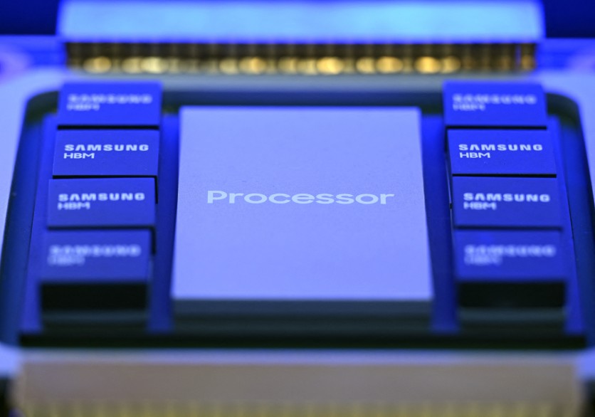
This picture taken on October 22, 2025 shows a mockup of a chipset featuring Samsung Electronics' high-bandwidth memory (HBM) technology on display during the 2025 Semiconductor Exhibition in Seoul. Jung Yeon-je/AFP via Getty Images
Samsung Electronics has published its first concrete performance targets for HBM5, its eighth-generation high-bandwidth memory, pegging the product at twice the overall capability of its current HBM4E generation — while introducing a named governing strategy called CUBE that frames 3D vertical integration as the company's answer to the limits of planar memory scaling.
Choi Jang-seok, vice president and head of the memory product planning team at Samsung Electronics, delivered the roadmap in a keynote at the Memory Executive Summit in Taipei on Tuesday, a pre-show forum held ahead of the SEMICON Taiwan 2026 main exhibition opens Wednesday at the Taipei Nangang Exhibition Center. The keynote marked the first time Samsung has articulated specific HBM5 performance targets relative to HBM4E, its currently sampling seventh-generation product.
What Samsung's CUBE Framework Actually Means for Memory Design
CUBE is Samsung's acronym for Capacity, Utilization, Bandwidth, and Efficiency — the four dimensions the company says define competitive leadership in AI memory. The Samsung 3D architecture strategy signals a philosophical shift: rather than competing primarily on die count, pin speed, or fabrication node in isolation, Samsung is centering its roadmap on how each vertical layer of a memory stack contributes to the system's overall performance per watt.
"We are no longer constrained by the size of the printed circuit board, because memory capacity can be increased by stacking components vertically, without making the board larger," Choi said during the CUBE strategy Choi keynote. "By dramatically shortening the distance between dies, we can create vertical data highways and significantly increase bandwidth."
The architecture that makes vertical highways possible is through-silicon via technology — TSVs for short. Each TSV is a vertical copper-filled hole etched through a silicon die, and an HBM stack contains thousands of them. The Samsung HBM TSV architecture means data traveling through a TSV crosses tens of micrometers rather than the millimeters a silicon interposer trace requires or the centimeters a printed circuit board trace demands. That compression in physical distance is what converts a structural change — stacking chips vertically — into a specific, measurable reduction in energy per bit transmitted.
"The ultimate goal of 3D architecture is to reduce the energy required to transmit a single bit of data," Choi said, "and Samsung is maximizing performance per watt by improving structural efficiency." This energy per bit design goal underpins the entire CUBE framework.
The CUBE framework applies this logic across Samsung's entire memory lineup — not just HBM for AI accelerators, but also NAND flash storage — making it a strategic architecture rather than a generation-specific product claim.
HBM5: First Concrete Targets Put Performance at 2x HBM4E
Samsung is developing HBM5 as the direct successor to HBM4E, whose Samsung HBM4E first samples reached major AI accelerator customers in late May 2026. The HBM4E specs and shipment dates show a stable pin speed of 14 gigabits per second (Gbps), scalable to 16 Gbps, with a single-stack bandwidth of 3.6 terabytes per second (TB/s).
Samsung's Samsung HBM5 performance targets are:
- Roughly twice the overall performance of HBM4E
- A 20 percent improvement in performance per watt
- A 20 percent reduction in thermal resistance
These numbers represent the clearest window yet into what AI system architects will have available when HBM5 reaches volume production, with the HBM5 volume production timeline currently projected around 2028. A 2x overall performance improvement over HBM4E's 3.6 TB/s per stack would place HBM5's bandwidth potential above 7 TB/s per stack — a figure that shapes the maximum achievable throughput of the AI accelerators it will attach to.
The two engineering choices driving those targets were already disclosed at earlier venues: HBM5's thermal architecture includes Heat Path Block, a structure embedded within the die stack that functions like a chimney, creating a dedicated heat-transfer path between the stacked DRAM dies and routing thermal energy away from the die-to-die interfaces. The Heat Path Block thermal architecture was validated on HBM4E products before its incorporation into the HBM5 plan — directly addressing the overheating failures behind the Samsung HBM3E Nvidia test failures that cost Samsung a generation of Nvidia business when its HBM3E chips failed qualification in 2024.
HBM5's base die — the logic layer at the bottom of the stack that manages communication with the host processor — will be manufactured on Samsung's in-house 2-nanometer foundry process, one full node below the 4-nanometer process used for HBM4 and HBM4E base dies. That Samsung 2nm HBM5 base die process node advancement is expected to improve power efficiency and processing throughput at the memory interface layer, and differentiates Samsung's approach from SK Hynix, which has relied on TSMC's 12-nanometer (nm) process for its HBM base dies.
How AI Systems Are Architected Shapes Whether HBM5 Matters to You
The significance of Samsung's HBM5 targets is specific to where AI performance is actually bottlenecked. Large language models and other AI inference workloads are memory-bandwidth-bound, meaning the limiting factor on how fast the model runs is how quickly data can move between memory and the compute chip — not how fast the chip itself computes. The AI memory bandwidth bottleneck explained — the "memory wall" constraint identified by Wulf and McKee in 1995 — has become the defining constraint of AI inference at scale.
HBM addresses the memory wall by replacing centimeter-scale printed circuit board connections with the micrometer-scale connections TSVs enable — compressing the distance data travels by three orders of magnitude. HBM4's 2,048-bit bus can move data in parallel across more than 2,000 simultaneous paths at once; the HBM vs DDR5 bandwidth comparison result is 2 TB/s or more per stack, far exceeding what any conventional DDR5 configuration can match.
For engineers specifying AI accelerators beyond Nvidia's current Vera Rubin platform — the generation targeting HBM4 — Samsung's HBM5 targets provide the planning ceiling for the following generation, tentatively aimed at Nvidia's Feynman platform expected around 2028. Whether Samsung qualifies HBM5 with Nvidia before or after SK Hynix does is the commercial question; the technical parameters disclosed in Taipei are what system designers need to model toward.
Read more: Samsung HBM5 Debuts at Computex: Nvidia's Endorsement Still Goes to SK Hynix
zHBM: Eight Times HBM4E, No Commercial Timeline
Samsung also presented an update on zHBM — the "zero-distance" concept it introduced at the Future of Memory and Storage (FMS) conference in Santa Clara in early August — at the Memory Executive Summit. The architecture eliminates the silicon interposer entirely by stacking HBM directly above the AI accelerator die, with TSV connections running vertically rather than across a horizontal substrate.
Samsung's zHBM thermal targets SEMICON Taiwan are:
- Eight times the performance of HBM4E
- Three times the performance per watt vs HBM4E
- A 75 to 90 percent reduction in thermal resistance vs HBM4E
The framing of those targets against HBM4E rather than HBM5 is notable: because HBM5 itself targets a 2x improvement over HBM4E, zHBM would deliver roughly four times the performance of HBM5, implying it represents a generation beyond HBM5 in Samsung's product sequence — a technology currently at concept stage with no production timeline confirmed.
"The key to 3D is not simply stacking components, but how each layer is utilized," Choi said. This Choi 3D layer utilization quote sums up the principle distinguishing zHBM from conventional stacking approaches. "Samsung is optimizing the placement of logic and memory to reduce data processing latency."
The engineering challenge zHBM faces is thermal. An AI accelerator die — which generates substantial heat during inference and training — placed directly below stacked HBM modules creates a combined thermal environment more difficult to manage than the current side-by-side interposer arrangement. The zHBM heat management challenge is that Samsung's concept presentation included a proposed heat-dissipation structure routing thermal energy outward through a separate path between the memory and accelerator, but no commercial-scale yield data exists to confirm this approach works at production volumes.
The longer-horizon implication if zHBM succeeds is structural: the silicon interposer that connects HBM to AI accelerators in every current design is one of the most capacity-constrained elements in AI chip manufacturing, with CoWoS packaging lead times constraints at TSMC's advanced packaging lines exceeding twelve months. An HBM architecture that eliminates the interposer requirement for memory-to-processor connections would carry consequences well beyond Samsung's own product line.
zNAND-O: Bridging Storage to AI Model Capacity Needs
Alongside the HBM roadmap, Samsung detailed zNAND-O — a high-capacity NAND flash product designed for the storage demands of large language models. The zNAND-O specs and targets show the product stacks four or eight V-NAND dies using through-silicon vias and targets:
- Ten times the bit density of DRAM
- Seven times the read bandwidth and power efficiency of conventional NAND storage
The zNAND-O 2028 sampling schedule has customer sampling set to begin in 2028. The product fills a tier between conventional SSDs and DRAM in the memory hierarchy — a zone that matters specifically for AI inference workloads, where model weights are large enough to exceed DRAM capacity but fast enough in access requirements to exceed what standard NAND can serve.
Read more: Samsung's zHBM Places Memory on Top of AI Chips; BV-NAND Shatters 400-Layer Barrier
Samsung's Market Position Makes the Roadmap Credible — and Contested
Samsung arrived at the Memory Executive Summit as the overall DRAM revenue leader: the Samsung Q2 2026 DRAM market share placed it at 39 percent in the second quarter of 2026, its highest level since 2024, ahead of SK Hynix at 26 percent and Micron Technology at 25 percent, according to Counterpoint Research. Samsung NAND TrendForce market share stood at 29.3 percent in the same period, according to TrendForce.
In HBM specifically, Samsung's position is more complicated. The SK Hynix HBM market share IDC data cited in SK Hynix's U.S. Securities and Exchange Commission filing shows SK Hynix held 56.4 percent of the global HBM market by revenue in the first quarter of 2026. Samsung recovered its overall DRAM lead during 2026 after conceding it to SK Hynix in 2025, but the HBM-specific gap — particularly in supply relationships with Nvidia — remains the defining competitive question heading into the HBM5 generation.
The SK Hynix CEO memory shortage forecast from Kwak Noh-jung holds that the memory chip shortage driven by AI infrastructure demand could persist through the end of 2030. That sustained demand environment gives Samsung a multi-year runway to execute its CUBE roadmap and narrow the HBM-specific gap.
All performance figures disclosed in Taipei are Samsung's own development targets, not independently audited measurements. HBM5 remains in pre-production; no customer qualification data is public. The CUBE framework is a strategic statement of Samsung's architecture direction, not a product specification sheet with verified results.
Frequently Asked Questions
What does Samsung's CUBE strategy actually stand for, and how does it differ from prior HBM development?
CUBE is Samsung's acronym for Capacity, Utilization, Bandwidth, and Efficiency — the four dimensions the company says should govern AI memory design. Prior HBM generations were optimized primarily around bandwidth and capacity as separate metrics, often at the expense of efficiency and thermal management. CUBE formalizes Samsung's shift toward 3D vertical integration as the governing principle: stacking components along the Z-axis rather than expanding the footprint on the circuit board. The CUBE strategy full framework covers both HBM products (HBM5, zHBM) and NAND storage (zNAND-O), framing them as parts of a unified architectural direction rather than separate product lines.
How much faster is HBM5 supposed to be, and why does that number matter for AI systems?
Samsung targets HBM5 to deliver roughly twice the overall performance of HBM4E, along with a 20 percent improvement in performance per watt and a 20 percent reduction in thermal resistance. If HBM4E delivers up to 3.6 TB/s of bandwidth per stack at peak, a 2x improvement would suggest HBM5 operating above 7 TB/s per stack. The HBM5 bandwidth per stack explained figure matters because AI inference workloads are memory-bandwidth-bound, not compute-bound: the rate at which the GPU can be fed model weights from memory sets the ceiling on how fast the model can run. HBM5 is targeted for volume production around 2028, aimed at AI accelerator generations that follow Nvidia's current Vera Rubin platform.
What is zHBM and why is it still a concept rather than a product?
zHBM places HBM stacks directly above the AI accelerator die rather than beside it on a silicon interposer, with through-silicon via connections running vertically between the two. The zHBM FMS 2026 concept architecture targets 8x the performance of HBM4E and 75 to 90 percent lower thermal resistance — but the technology faces an unsolved engineering challenge: a heat-generating AI accelerator die directly bonded to HBM stacks creates a thermal environment that current packaging technology has not resolved at commercial scale and yield. Samsung has presented conceptual heat-dissipation structures, but no production-ready solution has been demonstrated. zHBM has no announced commercial timeline.
Does Samsung's roadmap mean AI hardware will keep getting more expensive?
Not necessarily more expensive per unit of performance, but capacity will remain constrained. Samsung has indicated that long-term supply agreements could eventually reserve 60 to 70 percent of its memory production for AI datacenter customers, as covered in the Samsung AI memory supply agreements analysis, which concentrates available memory toward the highest-margin AI workloads. For buyers outside that tier — PC manufacturers, smartphone makers, consumer electronics companies — this means the remaining supply pool is smaller. The Samsung Galaxy MX operating loss in Q2 2026 illustrates the pressure: Samsung's own Galaxy mobile division posted an operating loss partly because elevated memory component costs, driven by the AI supercycle, could not be passed through to device buyers.

-
 C114 Communication Network
 -
 Communication Home
