
 Search

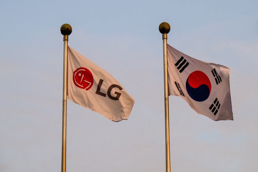
The company flag of LG and the national flag of South Korea flutter in the wind outside the LG Group's Twin Tower buildings in Seoul on September 9, 2025. ANTHONY WALLACE/gettyimages.com
South Korea's government-sponsored semiconductor program produced a striking industrial alignment on August 31: LG Electronics tapped chip designer CoAsia SEMI to develop two ultra-low-power AI IoT system-on-chips for its next-generation smart home appliances — with Samsung Electronics' foundry arm manufacturing them. That routing is unusual by any measure. LG and Samsung compete head-to-head across televisions, monitors, laptops, and home appliances, and LG has historically relied on TSMC — not Samsung — to fabricate chips even in prior government-funded programs.
The LG IoT chip deal was announced on the same day LG unveiled its ThinQ Claw AI home ecosystem and expanded AI Home platform at IFA 2026 in Berlin — a deliberate synchronization that places the chip deal squarely inside LG's publicly stated ambition to own the ambient AI home market. The silicon strategy and the consumer-facing vision arrived together because they cannot be separated: always-on AI appliances require always-on AI chips, and those chips do not yet exist at the price and power efficiency LG needs.
Cross-Rival Collaboration Rooted in Government Architecture
The partnership sits inside South Korea's K-On-Device AI Semiconductor Technology Development initiative, a program run by the Ministry of Trade, Industry and Resources with an overall semiconductor R&D budget of approximately ₩800 billion (approximately $585 million USD) running through December 2030. It spans AI semiconductor development across automobiles, IoT, home appliances, machinery, robotics, and defense, and counts Hyundai Motor, Doosan Robotics, Daedong, and Korea Aerospace Industries among its participating demand customers.
Within this program, the CoAsia SEMI–LG sub-project carries a dedicated development budget of ₩31 billion (approximately $22.7 million USD), with the full project timeline running from this year through December 2030. LG Electronics will define the chip specifications and steer the development direction. CoAsia SEMI will handle the chip architecture and optimize it for Samsung's manufacturing processes. Engineers from CoAsia NEXELL — a SoC-focused fabless subsidiary within the broader CoAsia Group — are also expected to contribute.
The stated engineering goal: a family of always-on sensing chips that dramatically reduce power consumption and bill-of-materials cost for LG's AI home platform, targeting an early position in what both companies see as the next competitive frontier for smart home products.
Why Samsung Foundry — and Why It Matters
The manufacturing decision is what has drawn the most attention from supply-chain observers. Industry insiders noted that LG Electronics has primarily used TSMC fabs even for government-funded chip projects. "Even for a government-funded project, it is unusual for LG Electronics to use Samsung Electronics' fab," one industry official told The Elec, the Korean semiconductor trade publication that first reported the deal.
The pivot matters because it is not merely cosmetic. CoAsia SEMI is an officially designated Design Solution Partner (DSP) of Samsung Foundry's SAFE partner ecosystem — meaning its chip designs are engineered from the ground up to Samsung's process specifications, using Samsung's qualified design flows, IP libraries, and manufacturing parameters. That process-specific optimization is not trivially portable: a chip architected to a Samsung process node is not the same chip as one architected to a TSMC process node, even if the logic functions identically. The engineering choices that minimize leakage current, optimize cell libraries, and reduce power in standby are foundry-specific. Once LG's IoT chip tape-out is complete on Samsung's process, future iterations will almost certainly return to the same foundry — not because of contractual lock-in, but because the design work has accumulated around Samsung's manufacturing environment.
This is how the Korean government's program may be doing something more durable than routing one chip order: it is building supply chain alignment through technical dependency, making Samsung Foundry the natural and lowest-friction choice for LG's AI home chip development over the four-year project window and beyond.
What Always-On AI Chips Actually Do — and Why They Require Custom Silicon
The engineering rationale for bespoke silicon begins with what "always-on sensing" demands at the circuit level. A smart home refrigerator that can detect when a door has been left open, recognize food inventory changes, or sense the presence of household members cannot accomplish these tasks by continuously running a general-purpose processor — the power draw would be prohibitive. Instead, the chip must exist in three states simultaneously: a deep sleep mode consuming microwatts or less, an event-triggered wakeup state consuming milliwatts, and a brief active inference state consuming perhaps tens of milliwatts when a sensor threshold is crossed.
Achieving this requires a specific architectural approach. The chip must implement multi-domain power gating — separate power islands for the sensor hub, the neural processing unit (NPU), and the main application processor, each independently controlled. The NPU itself must be capable of running lightweight inference models — keyword detection, presence sensing, anomaly detection — without waking the main CPU. And the entire design must operate at supply voltages low enough to minimize transistor leakage in idle states — a constraint that varies by foundry and process node.
General-purpose chips sourced from TSMC for LG's prior appliance lineup were not designed around these constraints. Custom silicon lets LG and CoAsia SEMI co-optimize the sensor integration, NPU architecture, and power gating specifically for the home appliance use cases LG has defined — and do so at the bill-of-materials cost scale that home appliances require. A smartphone chip that costs $20 in volume is economically incompatible with a washing machine that retails for $800.
Read more: Samsung Foundry Chiplet Platform Eyes 2027 Production for Robotics, Automotive AI
CoAsia SEMI: A Samsung Ecosystem Insider
The choice of CoAsia SEMI as chip designer is not incidental to the Samsung Foundry selection. CoAsia SEMI is a subsidiary of CoAsia Group, an Incheon-headquartered semiconductor and IT holding company that traces its origins to agency work with Samsung's System LSI and foundry businesses before formally establishing its DSP partnership with Samsung Foundry in 2019. The company is also an ARM Approved Design Partner (AADP), operates design centers across South Korea, the United States, China, Taiwan, Vietnam, Japan, and Germany, and has accumulated experience on Samsung's 4nm and 5nm process nodes.
In July 2025, CoAsia SEMI partnered with Korean AI chip startup Rebellions to co-develop a next-generation AI chiplet package as part of another national R&D initiative — demonstrating the firm's positioning as a repeat participant in Korea's government-mediated chip ecosystem.
"Based on our cooperation with LG Electronics, we will seek additional business opportunities in AI home products and various application markets," CoAsia SEMI CEO Shin Dong-soo said in the company's August 31 announcement.
What This Means for Samsung Foundry's Recovery
Samsung Foundry — the contract manufacturing business of Samsung Electronics — has spent the last two years clawing back from a difficult period. Yield problems at its 3nm process node drove key customers including Qualcomm toward TSMC, and the foundry division posted operating losses exceeding ₩2 trillion (approximately $1.5 billion USD) in the fourth quarter of 2024 alone. At its lowest point, some 4nm and 5nm production lines ran below 50% capacity utilization.
The recovery picture heading into the second half of 2026 is substantially improved. Utilization has climbed to the 70–80% range and Samsung has targeted full capacity utilization by the end of 2026, driven by demand for HBM4 base dies (fabricated on a 4nm process) and a growing roster of advanced-node orders. The foundry's 2nm process yield has reached approximately 60%, still below the roughly 70% threshold the industry considers sufficient for large-volume production, but improving.
TSMC, by comparison, held approximately 73% of the global pure-play foundry market in both Q1 and Q2 2026, according to Counterpoint Research data. Samsung held approximately 7% — a gap that has been widening, not narrowing, as TSMC's 2nm production ramp and AI chip demand continuously strengthen its leading position.
In this context, the LG deal — while modest in absolute development budget — carries meaningful symbolic weight. It places a domestic consumer electronics brand of genuine prestige on Samsung Foundry's roster for a government-aligned chip program, and it does so through the ecosystem mechanism (DSP-mediated design) that Samsung has been building specifically to attract smaller and mid-tier customers who cannot justify the engineering overhead of working directly with a foundry.
Read more: Samsung GaN Foundry Chips Flunk Heat Test While Rivals Already Ship at Scale
Korea's Broader On-Device AI Ambition
The K-On-Device AI program reflects South Korea's calculated effort to develop a domestically rooted AI semiconductor supply chain across sectors where on-device inference is becoming strategically important — automotive (Hyundai Motor), industrial equipment (Daedong), robotics (Doosan Robotics), and defense aerospace (Korea Aerospace Industries), as well as the consumer IoT and home appliance segment that LG anchors. The initiative is explicitly structured to connect domestic fabless designers, domestic foundries, and domestic demand companies — a supply-chain loop that keeps design fees, manufacturing revenue, and IP within Korea's semiconductor ecosystem.
For the home appliance segment specifically, the emphasis on always-on, ultra-low-power IoT SoCs reflects an industry-wide recognition that ambient AI — the ability of devices to continuously sense and interpret their environment without cloud connectivity for basic inference tasks — is where the next competitive differentiation will occur. LG's ThinQ Claw and AI Home announcements at IFA 2026 are the consumer-facing articulation of that premise; the CoAsia SEMI chip deal is the engineering substrate beneath it.
Whether the partnership yields chips that deliver a meaningful competitive edge over the four-year development window will depend on execution. But as a signal of how South Korean industrial policy can realign even entrenched competitive dynamics between rival conglomerates, the LG-Samsung-CoAsia deal is already a case study worth examining closely.
Frequently Asked Questions
Why is LG Electronics using Samsung Foundry instead of TSMC for these chips?
LG's pivot from its historical TSMC preference to Samsung Foundry is tied to the structure of South Korea's K-On-Device AI semiconductor program. The government initiative connects domestic chip designers (CoAsia SEMI is a Samsung Foundry Design Solution Partner) with domestic demand companies (LG) and domestic foundries (Samsung). An industry official told The Elec that the Samsung Foundry choice is unusual even by government-program standards, where LG has historically used TSMC. The practical consequence is significant: CoAsia SEMI's design work will be optimized for Samsung's manufacturing parameters, making Samsung the lowest-friction foundry for future LG IoT chip iterations as well.
How do always-on AI chips work in home appliances, and why do they need custom silicon?
Always-on sensing chips operate through a three-state power architecture: a deep sleep mode consuming microwatts while idle, a wakeup state triggered by a sensor event, and a brief active inference state where a neural processing unit runs a lightweight AI model to interpret the event. Keeping this cycle efficient at home appliance power budgets — where you cannot drain a battery or meaningfully increase electricity consumption — requires purpose-built chip architecture with multi-domain power gating and NPU cores optimized for the specific sensor combinations LG uses. General-purpose chips sourced from major foundries are not designed around these constraints, and they cost more per unit than high-volume appliance economics permit.
What does the K-On-Device AI program mean for Samsung Foundry's competitive standing?
The ₩800 billion (approximately $585 million USD) government program is structured explicitly to route chip orders through domestic foundries, giving Samsung Foundry access to a pipeline of domestic demand-customer projects that TSMC does not participate in. For a foundry working to rebuild its utilization from a low point where some lines fell below 50% capacity in 2024–2025, and currently targeting 100% utilization in H2 2026, institutionally guaranteed domestic projects provide a stable baseline of orders while the more competitive advanced-node customer wins continue to develop. The LG deal is small individually but represents the kind of domestic ecosystem anchoring that the Korean government program is specifically designed to create.
Is LG and Samsung now working together permanently?
This is a specific project partnership under a government-funded program, not a broad commercial alliance. LG and Samsung remain fierce competitors across TVs, monitors, laptops, and home appliances. The four-year chip development timeline extends through December 2030. Whether LG continues routing chip work through Samsung Foundry beyond that program will depend on whether the custom silicon delivers the performance, power, and cost advantages LG needs — and whether Samsung Foundry's process maturity at the relevant nodes justifies continued preference over TSMC.

-
 C114 Communication Network
 -
 Communication Home
