
 Search

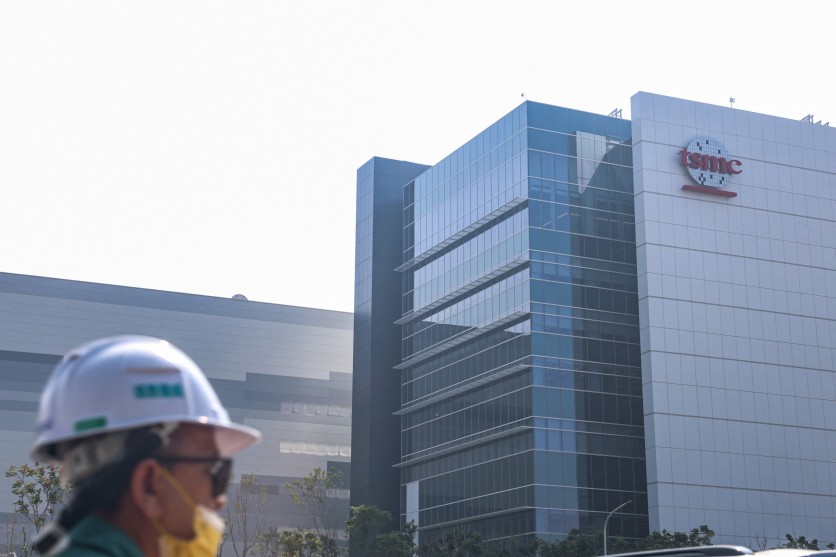
A worker walks past the 2-nanometer fabrication plant of the Taiwan Semiconductor Manufacturing Company (TSMC) at Nanzih Technology Industrial Park in Kaohsiung on December 23, 2025. I-Hwa Cheng/gettyimages.com
Taiwan Semiconductor Manufacturing Co. on Tuesday revealed that it is establishing a dedicated materials and equipment supplier campus inside Kaohsiung's Baipu Industrial Park — a facility designed not to manufacture AI chips but to compress the time it takes to qualify the next generation of materials needed to build them. The announcement, made at the 3D IC Global Summit on the eve of SEMICON Taiwan 2026, puts into concrete form a strategic recognition that has been building across the industry for months: that the binding constraint on advanced packaging throughput is no longer purely factory floor space, but the speed at which new materials, bonding processes, and inspection tools can be validated and brought to production.
The campus will be the first in Taiwan specifically dedicated to co-locating advanced packaging materials and equipment suppliers alongside TSMC's own engineers — a physical arrangement that, TSMC VP of Advanced Packaging Technology and Service Jun He said, is expected to improve packaging validation efficiency by 25 percent to 50 percent. That figure is not incidental. In a supply chain where CoWoS packaging slots run 52 to 78 weeks out, every week saved in qualifying a new underfill chemistry or bonding architecture translates directly into AI chips that can ship sooner.
What TSMC Is Actually Building in Kaohsiung
The Baipu site covers 3 hectares (approximately 7.4 acres) and will house two buildings with modular cleanroom facilities designed for reconfiguration as packaging technologies evolve — an architectural choice that prevents the campus from being locked into any single process geometry. Inside, small laboratories will serve as joint testing and R&D spaces for TSMC and its packaging materials and equipment partners, and a dedicated training center for advanced packaging specialists will operate alongside the technical facilities.
TSMC is developing the campus in partnership with Taiwan's Ministry of Economic Affairs and the Kaohsiung City government. He framed the goal at Tuesday's 3DIC Global Summit as building a world-class packaging talent base while connecting local suppliers directly with global supply chains.
The campus is explicitly not a production facility. It is a validation infrastructure — a purpose-built environment in which TSMC's engineers and the companies supplying the materials and tools they use can work through design iterations in the same physical space rather than shipping samples across borders and waiting weeks for results.
Why the Validation Gap Matters More Than the Capacity Gap
To understand why TSMC is building this, it helps to understand the specific problem it addresses — and why that problem is distinct from the CoWoS capacity gap that has dominated advanced packaging headlines for the past two years.
CoWoS — Chip-on-Wafer-on-Substrate — is TSMC's 2.5D advanced packaging technology that physically integrates AI logic dies with stacks of High Bandwidth Memory on a passive silicon interposer. The interposer carries microscopic copper-filled through-silicon vias, enabling memory bandwidth in the terabytes-per-second range that modern AI accelerators require. Every Nvidia GPU generation from H100 through Rubin ships on CoWoS; so does every AMD MI-series accelerator.
Expanding CoWoS capacity means building more cleanroom floor space — the work underway at Chiayi, Longtan, Tongluo, and Zhunan. But bringing that capacity to production yield requires qualifying the materials used in the process: the underfill epoxy that encapsulates and mechanically stabilizes the microbump connections between die and interposer; the flux chemistry that enables the solder reflow at temperatures around 250°C (482°F); the bonding tools that must place dies with sub-micrometer precision; and the inspection systems that verify every connection after bonding.
Qualifying each of these materials involves shipping samples to a supplier, receiving reformulated versions back, testing them in conditions that replicate the production environment, and iterating. When supplier facilities are in Japan, the United States, or Europe, each iteration takes weeks. By placing the supplier's equipment in the same building as TSMC's packaging engineers, in a cleanroom environment representative of production conditions, the iteration cycle can be compressed dramatically. TSMC's own supply chain localization program has demonstrated the effect in practice: in one documented case, relocating a Japanese supplier's production to Taiwan compressed the procurement cycle from 60 days to 20 days while improving transportation efficiency by 90 percent.
The 25 to 50 percent validation efficiency gain Jun He cited is this compression effect, applied to the highest-value materials qualification in the advanced packaging roadmap.
Why Iteration Distance Is the Next Frontier
TSMC has asked packaging materials and equipment suppliers to develop 5-micrometer-class microbump bonding technology for next-generation HBM packaging — a specification that represents a roughly twofold reduction from current production-class microbump pitches. At that scale, material properties interact with process parameters in ways that cannot be tested without production-representative equipment. A new underfill formulation that performs well on a supplier's lab bench may behave differently when dispensed in a TSMC-configured bonder under thermal cycling — and discovering that discrepancy in Japan or the United States costs weeks that, in a supply chain with 52-to-78-week lead times, carry real AI infrastructure consequences.
AT&S CEO Dr. Michael Mertin described the co-development relationship shift earlier this summer, telling Nikkei Asia that suppliers now "have to cooperate, you have to think, you have to have a joint roadmap." In traditional packaging supply chains, materials suppliers were largely commodity vendors that competed on cost and delivery. As AI chips integrate more chiplets onto single substrates at ever-denser configurations, the substrate and its associated materials are no longer passive carriers — they are active constraints on what the chip can do. Suppliers capable of forming co-development partnerships with TSMC at the design-specification stage will be structurally favored over arm's-length manufacturers.
The Baipu campus institutionalizes that co-development relationship in physical form.
Read more: SEMICON Taiwan 2026 Kicks Off: AI Chips' Bottleneck Is Wires Connecting Them
Baipu's Role in the Southern Technology Corridor
The Baipu Industrial Park campus is the latest node in a southern Taiwan semiconductor geography that TSMC and the Taiwanese government have been assembling at pace throughout 2025 and 2026. Baipu joins a southern Taiwan semiconductor corridor spanning Chiayi, Tainan, Kaohsiung, Pingtung, and Hsinchu science parks — a network that National Science and Technology Council Minister Wu Cheng-wen has described as the world's most comprehensive AI and semiconductor industry corridor.
Chiayi Science Park Phase 1 entered mass production in June 2026, with a groundbreaking ceremony held in July for the approximately 90-hectare (222-acre) Phase 2 site adjacent to it. Once all four Chiayi packaging facilities are operational, they are projected to generate annual output exceeding NT$300 billion (approximately $9.45 billion USD) and create more than 9,000 jobs. National Science and Technology Council Minister Wu Cheng-wen described the full corridor as the world's most comprehensive AI and semiconductor industry corridor, linking Chiayi, Tainan, Kaohsiung, Pingtung, Central Taiwan, and Hsinchu parks.
TSMC separately moved into Pingtung Science Park in June 2026 alongside seven supply chain partners. In the north, the Tongluo Science Park facility in Miaoli — an investment of approximately NT$90 billion (approximately $2.84 billion USD) — is on track for mass production in the third quarter of 2027.
Baipu is the first node in this corridor explicitly assigned a supplier-ecosystem validation function rather than a production function. Chiayi and Tongluo are adding CoWoS wafer starts. Baipu is adding the ability to qualify the next generation of materials that will determine what those wafer starts can build.
That is a structural distinction. The cluster of expertise, equipment, and tacit engineering knowledge that will form inside Baipu's modular cleanrooms is the kind of supply-chain advantage that cannot be replicated by investment alone — the kind that Porter's cluster theory and Marshall's agglomeration economics have documented as the durable competitive moat in technology-intensive manufacturing. TSMC's Arizona campus can replicate packaging capacity. It cannot replicate daily iteration between TSMC engineers and the specialty-materials suppliers refining bonding specifications in real time in the same building.
How Should an AI Infrastructure Buyer Read This?
TSMC's CoWoS capacity is expanding at a compound annual growth rate of more than 80 percent through 2027, with strong growth expected to continue through 2029, He said. Even so, analysts at TrendForce estimate a supply-demand gap of roughly 20 percent in 2026, narrowing to approximately 10 percent by year-end but persisting into 2027.
The Baipu campus does not directly add to that wafer-start count. What it does is compress the timeline on which new materials generations can be brought to production yield — which means that capacity additions at Chiayi Phase 2, Longtan, and the 14-reticle CoWoS architecture TSMC is targeting for 2028 can ramp faster than they otherwise would.
For enterprise AI buyers with procurement decisions to make now: CoWoS lead times of 52 to 78 weeks remain the operative constraint, and Baipu does not change that in 2026. The campus's effect on lead times will be felt in the 2027 to 2028 capacity ramp — the same window in which Chiayi Phase 2 and Tongluo are expected to contribute meaningfully to supply. Decisions made now about infrastructure commitments and hyperscaler partnerships should account for a supply chain that is structurally improving but remains supply-constrained through at least 2027.
The message from Kaohsiung is that TSMC understands the next constraint before the current one has resolved. As AI compute demands continue to outpace existing supply, TSMC is not simply building more of the same — it is restructuring the physical geography of how the next generation of packaging is developed.
Currency conversions in this article are approximate and based on exchange rates as of September 2, 2026.
Read more: Semiconductor Supply Chain Closes Fluoropolymer Gap: Nichias Builds PFA Tube Plant in Hsinchu
Frequently Asked Questions
What is the Baipu Industrial Park campus, and how is it different from TSMC's other packaging expansions in Taiwan?
The Baipu campus in Kaohsiung is specifically designed as a materials and equipment validation facility — a place where TSMC's packaging engineers and the companies supplying the materials and tools they use can work through design iterations in the same physical space. It is not a CoWoS production facility. TSMC's other recent expansions — Chiayi Science Park Phases 1 and 2, Longtan Phase 3, and the Tongluo Science Park fab (targeted for mass production in Q3 2027, with an NT$90 billion, approximately $2.84 billion USD investment) — are all adding wafer starts: physical CoWoS packaging capacity. Baipu adds something different: the ability to qualify next-generation materials faster, which in turn accelerates how quickly all of those capacity additions can reach full production yield. See the full TSMC announcement at Focus Taiwan.
Why does it take so long to qualify new packaging materials, and how does co-location help?
Qualifying a new packaging material — say, a new underfill epoxy for 5-micrometer-class microbump bonding — requires testing it under production-representative conditions: specific temperatures (solder reflow at around 250°C / 482°F), humidity levels, mechanical stress profiles, and bonding tool configurations. When a supplier's R&D lab is in Japan or Germany, each iteration cycle involves shipping samples internationally, having the supplier run tests on equipment that may be configured differently from TSMC's production environment, and waiting for reformulated samples to arrive. Each round takes weeks. When the supplier's equipment is in the same cleanroom building as TSMC's packaging engineers, that cycle compresses to days. TSMC's documented supply-chain localization program has shown this effect before: bringing one Japanese supplier's production to Taiwan reduced the procurement cycle from 60 days to 20 days. The 25 to 50 percent validation efficiency gain Jun He cited at the 3DIC Global Summit reflects this same compression logic applied to advanced packaging.
Does the Baipu campus reduce CoWoS lead times for buyers ordering AI chips today?
Not immediately. CoWoS lead times of 52 to 78 weeks reflect production capacity constraints, not materials qualification timelines. Baipu's effect on lead times will be felt in the 2027 to 2028 window, when new capacity additions at Chiayi Phase 2, Longtan, and Tongluo are ramping — and when next-generation packaging architectures (including the 14-reticle CoWoS configuration TSMC is targeting for 2028) will require qualified materials that have not yet been validated. Baipu is the infrastructure that speeds up that qualification, making those future capacity additions ramp-ready sooner than they would be otherwise. Enterprise AI buyers with procurement decisions that extend into 2027 and 2028 should factor that timeline into their infrastructure planning. TSMC's CoWoS capacity projections are detailed at Focus Taiwan.
What does the Baipu announcement mean for the geographic concentration of AI chip supply in Taiwan?
It deepens it. Baipu is not a geographic diversification move — it is an ecosystem-deepening move, designed to make Taiwan's packaging supply chain faster and harder to replicate elsewhere. The materials qualification expertise, the co-development relationships, and the tacit engineering knowledge that will form inside Baipu's modular cleanrooms are exactly the kind of advantage that cannot be moved to Arizona or Germany through a capital expenditure announcement. TSMC's Arizona campus is adding CoWoS capacity; it is not adding the supplier-ecosystem density that makes that capacity faster to improve. That asymmetry is the structural fact the Baipu campus reinforces: geographic concentration risk in Taiwan remains, and TSMC's response to the packaging bottleneck is to run faster in place rather than to distribute. More on Taiwan's semiconductor corridor geographic structure is available at Wikipedia.

-
 C114 Communication Network
 -
 Communication Home
