
 Search

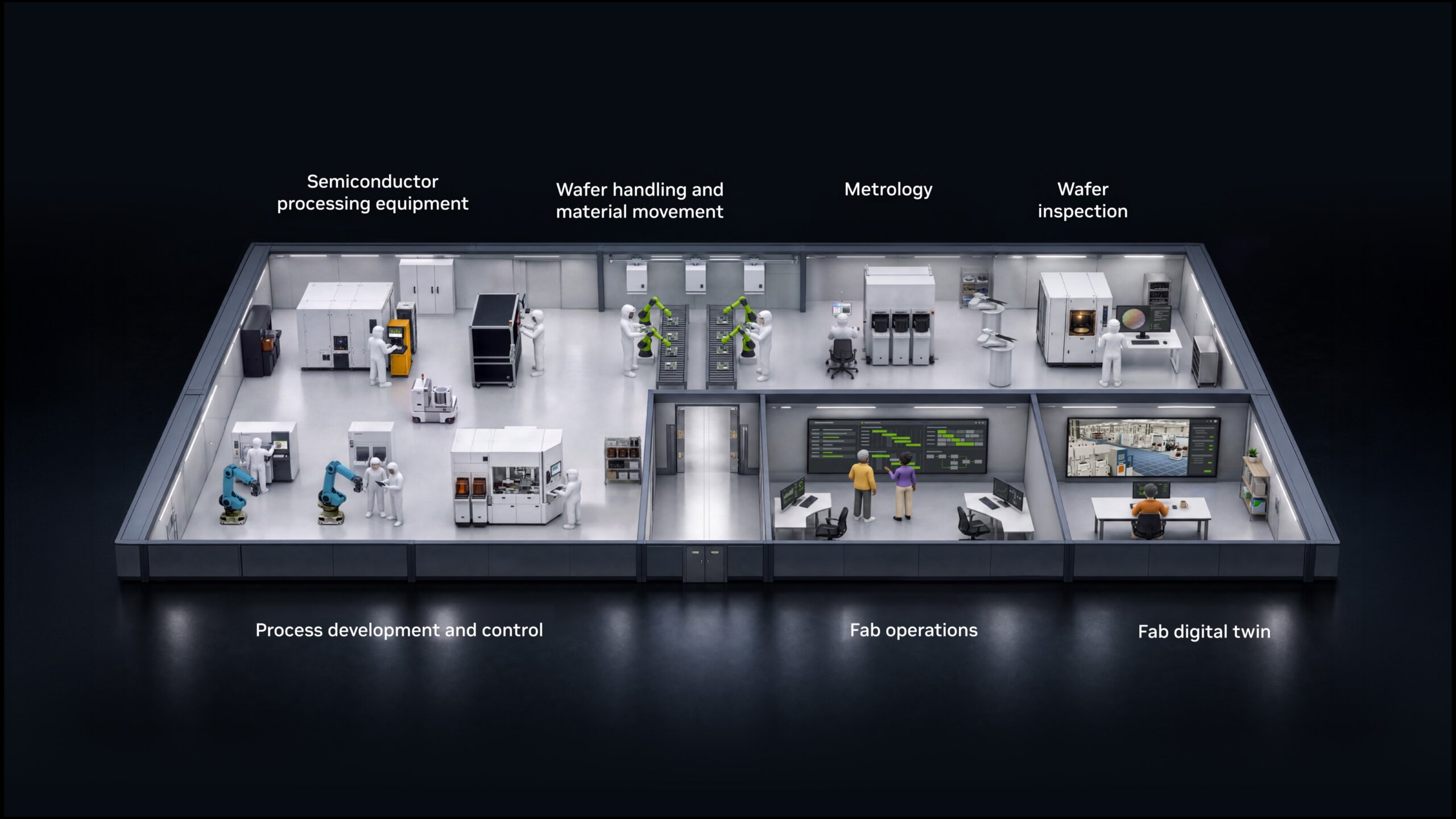
NVIDIA is expanding its accelerated computing and artificial intelligence software portfolio into semiconductor manufacturing, introducing new simulation, process modeling and inspection capabilities designed to improve advanced chip fabrication. Announced October 14, the initiative brings together NVIDIA CUDA-X libraries, AI models and digital twin technologies with Synopsys, Lam Research, KLA, Applied Materials, Siemens and Cadence.
The centerpiece is NVIDIA cuPotential, a GPU-accelerated library for atomic and molecular simulation. Early-access testing reported 2–3× acceleration compared with already GPU-optimized workflows. NVIDIA is positioning its GPU computing platform as an acceleration layer across semiconductor engineering, from materials and device simulation through etching, lithography, inspection and factory modeling.
Lam Research plans to incorporate NVIDIA NanoVDB into SEMulator3D, reporting up to 30× acceleration for selected wafer-etch simulations. KLA reported up to 50× acceleration for a normalized cross-correlation inspection kernel compared with earlier CPU implementations. Applied Materials reported up to 35× faster selected chamber simulations using NVIDIA technologies. These figures are vendor-reported, workload-specific benchmarks, not measured fab-wide throughput or yield improvements.
Key Developments
| NVIDIA AI-Defined Semiconductor Manufacturing | |
| cuPotential | Atomic and molecular simulation; 2–3× acceleration in early-access tests over GPU-optimized workflows. |
| Synopsys | cuEST and cuDSS integration for materials and device simulation. |
| Lam Research | NanoVDB and SEMulator3D; up to 30× on selected etch modeling. |
| KLA | NPP image-processing kernel; up to 50× against earlier CPU implementation. |
| Applied Materials | Omniverse and CUDA-X; up to 35× in selected chamber simulations. |
| Siemens / Cadence | Computational lithography, agentic engineering and simulation workflows. |
Analysis: GPU Acceleration Across the Semiconductor Manufacturing Lifecycle
The initiative extends NVIDIA’s accelerated computing stack into specialized engineering workloads that span atomic interactions, transistor behavior, manufacturing equipment and wafer inspection. The significance is not simply faster computation: reduced simulation time could enable engineers to test more materials and process configurations before deploying changes on production equipment.
The software vendors and equipment makers remain responsible for the specialized engineering tools. NVIDIA supplies GPU libraries, AI infrastructure and digital twin capabilities that can be integrated into those platforms. The reported benchmarks demonstrate acceleration on selected calculations but do not establish corresponding improvements in wafer yield, fab utilization, production cycle time or manufacturing cost.
As advanced logic, memory and packaging capacity expands for AI infrastructure, semiconductor process complexity and modeling requirements are increasing. The commercial impact of AI-defined fabs will ultimately depend on measured factory-level results.
Company Profile: NVIDIA
| NVIDIA | |
| Headquarters | Santa Clara, California |
| CEO | Jensen Huang |
| Platforms | CUDA-X, cuPotential, cuLitho, cuEST, cuDSS, NanoVDB, NPP, Omniverse |
| Markets | AI Infrastructure · Semiconductor Engineering · Data Centers |

-
 C114 Communication Network
 -
 Communication Home
