
 Search

Sedex.org
South Korea's two AI memory titans opened the country's largest semiconductor trade show on Wednesday morning with side-by-side booths, competing prototypes, and rival theories about what the next wave of artificial intelligence will actually need most from its memory chips.
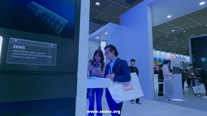
Samsung Electronics and SK Hynix both filled prominent floor space near the entrance to COEX Convention Center's Halls C and D at SEDEX 2026, record-largest edition, the 28th Korea Semiconductor Industry Association (KSIA) annual show. The 2026 edition drew 300 companies, 888 booths — roughly 70 more companies and 230 more booths than last year, making it the largest edition in the show's history.
The competitive intensity on that floor maps onto a specific engineering divergence. Samsung's HBM4 is built on its sixth-generation 1c DRAM — a 10-nanometer-class node one generation more advanced than what rivals are using — and stacks 12 dies high. SK Hynix's HBM4 uses a more mature 1b DRAM process, a fifth-generation 12nm-class node, but stacks 16 dies for more capacity. These are not cosmetic differences. They reflect two distinct bets about where AI infrastructure is heading.
Read more: SK hynix Orders Hanmi TC Bonder 4.5 Griffin for HBM4: First Griffin Contract Worth $28.7M
What Makes Two Memory Stacks an Engineering Argument
To understand why this matters, it helps to understand what happens inside an HBM4 chip. High Bandwidth Memory stacks multiple DRAM dies vertically, connecting them with Through-Silicon Vias — microscopic copper pillars drilled through each die — and bonding them under heat and pressure in a process called thermal compression bonding (TCB). The result is a memory cube that sits directly beside an AI processor on a silicon interposer, moving data across a bus that is 2,048 bits wide — double the width of the previous generation — at speeds of up to 2 terabytes of data per second at the JEDEC baseline, versus the narrow buses on conventional laptop or server memory.
Samsung's 1c DRAM process gives its HBM4 a speed advantage. Its chips achieve a consistent 11.7 gigabits per pin, and the company says that can reach 13 Gbps in optimized configurations, translating to 2.8 terabytes per second of total bandwidth per 12-layer stack. By applying a 4-nanometer logic process to its base die — the control layer at the bottom of the stack — Samsung brought the precision engineering of leading-edge logic chips into the memory business. "Instead of taking the conventional path of utilizing existing proven designs, Samsung took the leap and adopted the most advanced nodes like the 1c DRAM and 4nm logic process for HBM4," said Hwang Sang-joon of Samsung, head of memory development at Samsung Electronics, when the company announced its first commercial shipments.
SK Hynix deliberately did not race Samsung to the 1c process for its current HBM4 generation. Instead, it piled on more dies. At SEDEX 2026, the company displayed a full-scale model of its 16-high HBM4 stack — four layers taller than Samsung's offering — and the difference shows up directly in capacity. A 16-layer SK Hynix stack holds 48 gigabytes of memory; Samsung's 12-layer holds 36 gigabytes. SK Hynix has framed this as a strategic choice, not a lag. When Samsung announced its 1c-based product, SK Hynix responded that its HBM4 met performance requirements regardless — even based on the 1b process used in its current products — a comment widely read in Korea as a direct rebuttal of Samsung's performance framing.
Why Architecture Matters: Training vs. Inference
Here is the unstated argument beneath the booth rivalry: Samsung and SK Hynix have made opposite bets on which AI workload will dominate the next generation of data center spending.
AI training — teaching models from scratch on massive datasets — is the workload that made HBM famous. Training is bandwidth-hungry: the GPU needs to move model weights constantly, in massive parallel bursts, and raw data transfer speed is the primary limit. Samsung's faster-per-pin 1c DRAM approach is well-suited to this use case.
But AI inference — running trained models to generate responses for millions of users — is increasingly where the money is flowing, and inference has a different bottleneck. Every time a large language model processes a long conversation or a complex multi-step request, it must store in memory what are called key-value cache entries: vectors that represent every previous token in the exchange, so the model doesn't have to recompute them. This KV cache can become enormous. A single inference cluster serving thousands of simultaneous long-context conversations can exhaust its HBM capacity long before it exhausts its bandwidth — triggering slowdowns as data spills into slower memory tiers.
SK Hynix President Ahn Hyun made exactly this argument in his opening keynote at SEDEX, which he titled "Asking About the Direction of Memory Innovation in the AI Era." He forecast that the industry will need to scale AI infrastructure roughly 20-fold by 2030 indexed to today's performance baseline, and identified the KV cache overflow problem — driven by longer context windows, more complex agent tasks, and sheer request volume — as the central bottleneck. A 16-high 48GB stack gives inference clusters meaningfully more room before they hit that wall. SK Hynix's bet is that capacity will be the deciding criterion.
Neither bet is wrong on its own terms. But they cannot both be optimized simultaneously — at least not yet. Stacking 16 dies while also using a more advanced DRAM process requires passing the yield risks of both through each bonding layer, and the JEDEC 775-micrometer height limit constrains how much stack height is available. SK Hynix chose mature manufacturing with maximal height; Samsung chose the most advanced process with proven 12-layer execution. The market will answer which theory was right.
How HBM Chips Get Built: The Equipment Bottleneck Nobody Discusses
No company builds HBM stacks without thermal compression bonding equipment, and one company dominates that market: Hanmi Semiconductor's TC Bonder machines hold the dominant share of global HBM bonding tool supply, making Hanmi a South Korean equipment maker whose position in the supply chain rivals the memory companies themselves. Hanmi exhibited at SEDEX 2026 and drew substantial industry attention both for its current TC Bonder 4 system — now in mass production supply — and for its next-generation Wide TC Bonder, scheduled for commercial release in 2027.
The TC Bonder applies calibrated heat and pressure to bond each DRAM die in a stack, creating the precise metallic connections between through-silicon vias. Every layer adds its own yield fraction to the multiplication. At 16-high stacking, a 97% per-layer yield — already demanding — produces a finished stack yield below 61%. Maintaining acceptable production economics at that height requires not just good equipment but exceptional process control, which is why Hanmi's bonding tool precision improvements directly enable SK Hynix's stacking strategy. In June of this year, SK Hynix signed a contract with Hanmi worth ₩44.2 billion (approximately $33 million USD) for TC Bonder 4.5 Griffin units upgraded to SK Hynix's specific production specifications at the Cheongju facility.
Hanmi also showed a prototype of its Wide TC Bonder at SEDEX, designed to handle larger DRAM die sizes planned for future HBM generations. Larger dies allow wider I/O interfaces and more Through-Silicon Vias, increasing total bandwidth — but they also demand new bonding precision that existing equipment cannot achieve at production yields. The Wide TC Bonder represents the enabling tool for the generation after HBM4E.
Beyond HBM: SK Hynix's Vision of a Multi-Tier Memory Hierarchy
SK Hynix used its SEDEX 2026 keynote to present a roadmap that extends well beyond its current HBM4 products. Ahn Hyun outlined a three-part future for AI memory architecture.
The first tier remains HBM, but evolving toward "custom HBM" — variants in which a customer-specific logic layer is embedded directly into the base die, tailoring the memory architecture to each AI accelerator customer's specific needs. SK Hynix showed its 16-high HBM4 and roadmap artwork for HBM4E at SEDEX, while an autographed HBM wafer bearing Nvidia CEO Jensen Huang's signature — from his Korea visit confirming HBM4 qualification in June, during which he confirmed all three major memory makers had completed HBM4 qualification and entered mass production — occupied a prominent display position.
The second tier in Ahn's framework is 3D Stacked DRAM: a technology that places DRAM dies directly on top of GPU and neural processing unit chips, dramatically reducing the distance data must travel compared to sitting across an interposer. The shorter the electrical path, the lower the latency and power — a crucial consideration as AI models grow.
The third tier, and perhaps the most consequential announcement at SEDEX 2026, is High Bandwidth Flash: SK Hynix's proposal for a NAND-based memory tier packaged in an HBM-compatible form factor with a bus interface designed to work alongside HBM in an AI accelerator stack. HBF cannot match HBM4's raw bandwidth — SK Hynix estimates it will deliver roughly half — but it offers more than ten times the capacity per package, at substantially lower cost per gigabyte. The target use case is precisely the KV cache overflow problem Ahn described: when an inference cluster runs out of HBM capacity for active KV caches, HBF would provide a high-bandwidth but high-capacity tier to absorb the overflow, rather than forcing data down to much slower NVMe drives. SK Hynix announced at SEDEX that it plans to finalize the technical standard for HBF in January 2027.
Samsung's Counter-Thesis: Integration Beats Specialization
Samsung organized its SEDEX 2026 booth around the theme "Architecting AI Systems," with a message designed to distinguish it from SK Hynix in a dimension other than memory speed alone. DS Division CTO Song Jai-hyuk, who simultaneously chairs KSIA and presided over the opening ceremony, articulated Samsung's central argument during his SEDEX keynote on semiconductor integration: "Samsung is the only company in the world that covers DRAM memory, logic chips, CMOS image sensors, and packaging."
The practical implication is that Samsung can build HBM4's base die on its own 4nm foundry process, co-optimize the memory and logic layers in ways that external foundry customers cannot easily replicate, and integrate HBM into broader AI system packaging solutions from a single source. SK Hynix outsources its HBM4 logic base die to TSMC — which gives it access to TSMC's proven 12nm node but removes Samsung's vertical-integration advantage.
Samsung's booth displayed several products beyond its flagship HBM4. LPDDR-PIM — low-power DDR memory with processing-in-memory logic integrated into the die — reduces the need to ship data repeatedly to a GPU for simple operations. zHBM, a future architecture, would stack HBM directly on top of an AI processor to reduce interconnect latency further. The company also showed its 2.3D Cube-E and 3D Cube-H advanced packaging platforms, aimed at the heterogeneous integration market: co-packaging memory and logic dies horizontally or vertically into a single AI accelerator package.
Samsung displayed its HBM4E prototype under glass — the seventh-generation product it unveiled at Nvidia's GTC conference earlier this year — and confirmed the roadmap from 1c HBM4 through HBM4E and toward future hybrid-bonded memory generations.
Opening Keynotes: Three Visions for Silicon Intelligence
The SEDEX 2026 opening ceremony delivered three keynote addresses to a packed hall on the first morning. SK Hynix's Ahn Hyun delivered the lead speech, titled "Asking About the Direction of Memory Innovation in the AI Era," laying out the KV cache capacity thesis and SK Hynix's full memory hierarchy roadmap.
Shin Dong-ju, CEO of Mobilint — a Seoul-based fabless chip startup building neural processing units for edge inference — followed with a presentation titled "AI Semiconductors Opening the Era of Physical AI." Shin argued that the next wave of semiconductor demand will come not only from hyperscale data centers but from robots, autonomous vehicles, and industrial systems that cannot rely on a cloud connection: a future that demands chips capable of inference at the edge without constant network overhead.
Professor Park Seung-bae of the State University of New York closed the keynote session with "Challenges and Opportunities in the Era of Future Computing," surveying near-term architectural transitions from conventional computing toward near-memory and in-memory computing models, and cautioning that process node scaling alone cannot deliver the performance gains that AI workloads demand.
The Wider Context: Rubin, ASML, and the Race's Stakes
The rivalry on the SEDEX floor cannot be separated from the supply chain competition now playing out in AI accelerator design. Both Samsung and SK Hynix have been selected as HBM4 suppliers for Nvidia's Vera Rubin AI accelerator platform, which is expected to supersede the current Blackwell generation. SK Hynix currently holds approximately 62 percent of the global HBM market by shipment volume, according to Counterpoint Research data from the second quarter of this year. Counterpoint projects Samsung's share will expand to over 30 percent as HBM4 production ramps through 2026 and into 2027.
The capital spending context suggests neither company is slowing down. ASML, the Dutch company that makes the extreme ultraviolet lithography equipment that both Samsung's 1c DRAM process and SK Hynix's future roadmap depend on, this morning reported record quarterly net sales of €11.7 billion (approximately $13.1 billion USD) for the third quarter of 2026 — a result that signals the semiconductor industry's largest tool purchases extend forward through at least 2030. The customers driving those orders are, in no small part, the same Korean memory makers competing on the SEDEX floor.
Full Schedule Through October 16
SEDEX 2026 extends beyond the exhibition floor through Friday, with a full program of technical conferences, standards forums, and industry workshops.
On Thursday, the JEDEC AI Memory Forum — formally titled the Industry Forum on AI Memory Architectures, Testing, and Ecosystem Readiness — will convene at 1 p.m. Korean time (midnight ET) to present updates on HBM standards, including the timeline for formalizing SK Hynix's proposed HBF prefetch standard, alongside LPDDR6 and packaging interface specifications. The forum is likely to draw significant attention from memory engineers watching whether SK Hynix's January 2027 finalization target for the HBF standard will be endorsed or shifted. A Semiconductor Market Outlook Seminar will run simultaneously, with industry analysts presenting demand forecasts for AI memory and advanced packaging through 2030.
Also on Thursday, a 9th Semiconductor Industry-Academia-Research Exchange Workshop begins, presenting research from Korean university and national laboratory engineers on DRAM scaling, new memory materials, and computing architecture. A Semiconductor Talent Recruitment Fair brings 18 companies together with 433 registered job seekers across both Thursday and Friday.
Friday's headliner is a full-day conference titled "Semiconductors That Power Humanoids," exploring the chip architecture and memory requirements for humanoid robots — custom neural processing units, edge AI memory, low-latency sensor-to-actuator interfaces, and the supply chain implications of embodied AI scaling. As major robotics companies accelerate humanoid deployment timelines, this session is, in many ways, the exhibition's most forward-looking event and a preview of the next wave of specialty semiconductor demand after data center HBM.
Exhibition hours run 10 a.m. to 5 p.m. Korean time (9 p.m. to 4 a.m. ET) Wednesday and Thursday, and 10 a.m. to 4 p.m. Korean time (9 p.m. to 3 a.m. ET) Friday. General admission is ₩20,000 (approximately $15 USD), free for pre-registered visitors.
(Exchange rate as of October 14, 2026; all KRW and EUR conversions are approximate.)
Frequently Asked Questions
What is HBM4 and why does it matter for AI?
HBM4 is the sixth generation of High Bandwidth Memory, a type of DRAM that stacks multiple memory dies vertically using tiny copper columns called through-silicon vias, then bonds them directly beside an AI processor chip. The result is a memory package that moves data across a JEDEC-specified 2,048-bit bus — double the previous generation — at speeds of up to 8 gigabits per second per pin at the base specification, with Samsung and SK Hynix both shipping products above 11 Gbps. This matters for AI because training and running large language models demands memory bandwidth far beyond what conventional server memory can provide; HBM4 is the technology that lets an Nvidia AI accelerator process the data volumes those models require.
What is the difference between Samsung's and SK Hynix's HBM4 approaches?
Samsung built its HBM4 on a sixth-generation 1c process — its approximately 10-nanometer-class manufacturing node — and stacks 12 dies high. This gives Samsung's product an advantage in raw data transfer speed: 11.7 gigabits per second per pin consistently, and up to 13 Gbps in some configurations. SK Hynix built its HBM4 on the slightly older 1b process for yield stability (fifth-generation, approximately 12nm class), which it chose for proven yield, but stacks 16 dies high — giving each package 48 gigabytes of capacity versus Samsung's 36 gigabytes. The underlying argument: Samsung's speed advantage suits AI training workloads; SK Hynix's capacity advantage suits AI inference at scale, where longer conversations and complex reasoning tasks create large "key-value caches" that can fill available HBM memory before bandwidth becomes the limit.
What is High Bandwidth Flash, and why did SK Hynix announce it at SEDEX?
High Bandwidth Flash is SK Hynix's proposal for a NAND-based memory tier packaged in an HBM-compatible form factor. Unlike HBM, which uses DRAM, HBF uses flash memory — the same technology inside SSDs — to offer more than ten times the storage capacity of an HBM4 stack at roughly half the bandwidth and a substantially lower cost per gigabyte. The target use case is AI inference clusters that run out of fast HBM memory to store active key-value caches for long-context conversations: HBF would absorb that overflow at far higher bandwidth than existing NVMe drives. SK Hynix plans to finalize the HBF technical standard in January 2027.
Who makes the equipment that stacks HBM memory chips, and why does it matter?
Thermal compression bonding equipment — machines that apply calibrated heat and pressure to bond individual DRAM dies as they are stacked — is the critical manufacturing tool for all HBM production. Hanmi Semiconductor's market dominance in TC bonder supply means the South Korean equipment maker holds the dominant share of the global HBM TC bonder market, making it a pivotal link in both Samsung's and SK Hynix's supply chains. Hanmi signed a ₩44.2 billion SK Hynix contract in June (approximately $33 million USD) for TC Bonder 4.5 Griffin units upgraded to SK Hynix's 16-high production specifications. The company also showcased a prototype of its next-generation Wide TC Bonder at SEDEX 2026, designed for the larger DRAM die sizes planned for post-HBM4 generations — with commercial release targeted for 2027. Higher stacking requires increasingly precise bonding, and every additional layer multiplies yield challenges: Hanmi's equipment precision is as much a competitive variable in the HBM4 race as the DRAM process nodes themselves.

-
 C114 Communication Network
 -
 Communication Home
