
 Search

Lginnotek.com
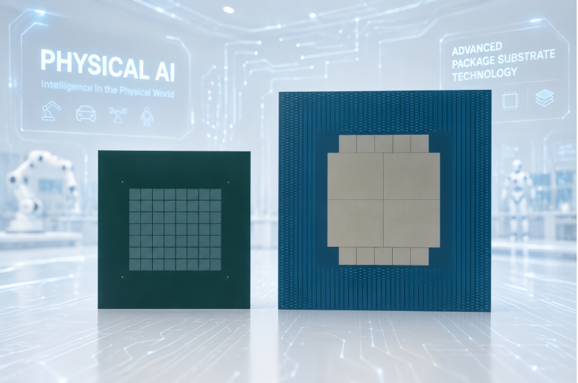
The race to build the layer beneath tomorrow's AI chips arrived at Korea's largest semiconductor packaging industry show Wednesday, when Samsung Electro-Mechanics and LG Innotek unveiled competing next-generation substrate technologies at KPCA Show 2026 in Songdo, Incheon — a direct challenge to the Japanese and Taiwanese incumbents who still control roughly 70 to 75 percent of the global advanced packaging substrate market.
KPCA Show 2026, now in its 23rd year, opened Wednesday at Songdo Convensia and drew roughly 350 domestic and international companies. The three-day event, organized by the Korea PCB and Semiconductor Packaging Industry Association, is Korea's flagship trade exhibition for printed circuit boards and semiconductor packaging — and this year it hosted the most consequential head-to-head display of next-generation substrate technology the Korean industry has staged.
What FC-BGA Substrates Actually Do — And Why AI Chips Are Breaking the Rules
To understand what was displayed at Songdo, it helps to understand what a package substrate actually does. Sitting between a processor die and the server's main circuit board, an FC-BGA — flip chip ball grid array — substrate routes power, high-speed signals, and heat through layers of microscopic copper wiring. In a standard consumer chip, the task is modest. In a next-generation AI accelerator, it is anything but.
As AI processors have grown in size and complexity — Nvidia's latest Rubin Ultra die, for instance, spans roughly double the footprint of its Blackwell predecessor — the substrates beneath them have had to scale accordingly. That scaling requires more wiring layers, finer copper traces, higher numbers of connections (called vias and bumps), and all of this at a physical scale where heat-induced warpage becomes the primary manufacturing enemy.
Warpage is what happens when different materials in a substrate expand at different rates during the high-temperature processes of manufacturing and chip attachment. Organic laminate substrates — the type used in most FC-BGA packages today — have a thermal expansion coefficient roughly six times higher than silicon. At small package sizes, this mismatch is manageable. At the 100mm-class sizes that next-generation AI accelerators demand, it becomes a primary yield-killer.
Read more: AI Supply Crisis Moves Upstream: Advanced Packaging Becomes the Binding Constraint
Substrate availability has emerged as a genuine first-order constraint on AI chip output, industry analysts say. Japan's Ibiden and Shinko Electric Industries together control an estimated 70 percent of the high-end FC-BGA substrate market, with the remainder split among a small number of suppliers — including Taiwan's Unimicron, Austria's AT&S, and the two Korean companies on display at KPCA Show this week. Expanding factory lines for these substrates takes 18 to 24 months due to long equipment lead times, which is why the competition playing out in Songdo has consequences far beyond Korea's domestic industry.
LG Innotek: Going Bigger, and Going Deeper Inside the Substrate
LG Innotek's exhibit centered on two technologies that collectively represent a step change in how much an FC-BGA substrate can do.
The company's headline reveal was what it called an ultra-large, 100mm-class FC-BGA substrate for AI accelerators — the first time LG Innotek has shown a physical sample of this size. At roughly 40 percent larger in surface area than the 85mm-class substrates it currently produces, the new substrate uses high-density circuits and an elevated layer count to link GPUs, NPUs, and memory within a single package. The engineering challenge is significant: at this size, organic substrates tend to warp during assembly, reducing the yield of chips successfully bonded to them. LG Innotek says it has managed that challenge and targets mass production beginning in 2027.
Equally significant — and more technically novel — was LG Innotek's display of FC-BGA substrates with embedded silicon capacitors, shown publicly in production-ready form for the first time at KPCA.
A capacitor's job in a chip package is to deliver clean, stable power to a processor that switches at billions of cycles per second. In most substrates today, capacitors are mounted on the substrate's surface, connected to the chip through metal traces that introduce inductance — a resistance to rapid changes in current. That inductance creates voltage ripple, which at the gigahertz frequencies where AI chips operate can degrade performance and reliability. Moving the capacitors inside the substrate — embedding them in either the core layer or a buildup layer — dramatically shortens the power delivery path. That shorter path lowers equivalent series inductance, smoothing out the voltage fluctuations that otherwise tax AI chip power circuits.
LG Innotek displayed two structural variants of the embedded design: one with silicon capacitors in the substrate's core layer, accommodating thicker and higher-capacitance components; and one with thinner capacitors in the buildup layer to minimize the package's overall height. An LG Innotek official said at the show that the placement and specifications of the capacitors can be varied to match different chip and substrate designs.
"In the past, substrates simply served as a medium for transmitting signals, but they are now evolving to provide functionality themselves by incorporating silicon capacitors, inductors, and other components," the official said. "Moving components from the substrate surface to the inside gives customers greater design flexibility and enables thinner products."
The company has been developing embedding technology for roughly a decade, beginning with multilayer ceramic capacitors inside flip-chip chip-scale packages. It first showed FC-BGA embedding with silicon capacitors in 2024 and began incorporating it in mass-produced products the following year. LG Innotek is also developing the capability to embed active components and signal bridges inside FC-BGAs — a more ambitious step that would allow the substrate itself to participate directly in routing signals between chips.
Also on display were LG Innotek's glass substrate development (targeting mass production in 2028) and Econova, which it described as the world's first smart integrated circuit tape substrate to achieve high performance without plating with precious metals such as palladium or gold — a feature drawing interest in European markets as environmental regulations on industrial precious-metal use tighten.
The company's Package Solution Business posted first-half 2026 revenue of ₩935.6 billion (approximately $700 million) — an 18 percent increase year over year — with operating profit rising 94 percent to ₩99.6 billion (approximately $74 million).
Samsung Electro-Mechanics: Breadth Across Five Substrate Types
Samsung Electro-Mechanics took a different approach, displaying the widest substrate portfolio it has publicly assembled in one place: five distinct types targeting AI accelerators, servers, data centers, mobile devices, and automotive electronics.
At the front of its booth were its 2.5D and 2.1D packaging substrates — its primary pitch to AI datacenter customers.
The 2.5D offering links multiple high-performance chips on a single substrate at high density. In a 2.5D package, the GPU die and high-bandwidth memory stacks sit side by side on a passive silicon interposer — a thin chip-like layer studded with through-silicon vias carrying data at terabytes per second — and the full assembly then mounts on the FC-BGA substrate. Samsung Electro-Mechanics reduced large-substrate warpage while maintaining the ultra-fine circuits, vias, and high bump counts needed for maximum data transfer speeds and power efficiency.
The 2.1D variant takes a different architectural path, connecting chips directly through fine circuitry built into the substrate layer itself — without the silicon interposer. Eliminating the interposer reduces cost and complexity, and sidesteps dependence on TSMC's CoWoS advanced packaging lines, which carry 52 to 78 week lead times. The tradeoff is lower interconnect bandwidth density than a 2.5D configuration, but for AI inference workloads — which are less bandwidth-intensive than training — it represents a practical alternative.
Glass substrates were the most forward-looking exhibit from SEMCO. The company presented technology for forming microscopic channels in glass and filling them with metal — a process called through-glass via formation — alongside precision surface processing technology. Glass substrates, used in place of the standard organic laminate core, offer a coefficient of thermal expansion roughly six times lower than organic materials, closely matching that of silicon. The result is dramatically lower warpage at large package sizes, and the ability to hold wiring pitches below two microns that organic materials cannot reliably sustain.
Samsung Electro-Mechanics has been running a glass substrate pilot production line at its Sejong facility and is targeting volume production after 2027. The company has already supplied glass substrate samples to customers including Apple and Broadcom for validation testing. In July 2026, it finalized a ₩480 billion (approximately $359 million) joint venture — named GlaSSEM — with Dongwoo Fine-Chem, a subsidiary of Japan's Sumitomo Chemical, to produce the glass core material in-house from the second half of 2027.
Rounding out the SEMCO lineup were automotive FC-BGA substrates engineered for the extreme temperature ranges, humidity exposure, and vibration demands of vehicle electronics, and ultra-thin chip-scale package substrates using a coreless structure for datacenter blade servers and mobile devices.
Read more: Samsung Electro-Mechanics Forms $310 Million Glass-Core Venture With Sumitomo Unit
Who Holds the Market — And What These Debuts Are Really About
Both Samsung Electro-Mechanics and LG Innotek entered the AI substrate business as challengers, not incumbents. Japan's Ibiden and Shinko Electric, supplemented by Taiwan's Unimicron, built their market positions over decades of patient manufacturing investment and customer qualification. Ibiden alone holds the single largest share of high-end AI server FC-BGA supply, and in February 2026 it announced a ¥500 billion capital expenditure plan — with customers including Nvidia, Intel, and hyperscalers co-funding the expansion through advance payments. Intel, AMD, and Nvidia have collectively co-funded roughly 50 percent of the expansion capital at their top four substrate suppliers — a pattern that, when customers behave this way, signals they believe they have no practical alternative.
The KPCA Show displays are Samsung Electro-Mechanics' and LG Innotek's argument that there is, in fact, an alternative — or that there will be one by 2027. That argument is already being made with balance sheets as well as engineering samples. By the first half of 2026, SEMCO's semiconductor substrate lines were running at approximately 89 percent utilization, while LG Innotek's had reached around 94 percent — essentially full capacity, with demand exceeding supply.
The market's response to that scarcity looks increasingly like the memory chip sector. "Looking at global substrate makers, most have already secured advance orders based on long-term agreements through 2029," Cho Ji-tae, head of LG Innotek's Package Solution Business, said at an earlier briefing this year. "These are not simple verbal arrangements but binding contracts with strong penalty clauses." LG Innotek noted that its over-100mm FC-BGA is being jointly developed with North American customers who have made financial commitments to secure production capacity. SEMCO, similarly, has most of its high-end FC-BGA output already allocated.
The substrate market was valued at an estimated ₩15.2 trillion (approximately $11.4 billion) in 2024, with research firm Prismark projecting growth to ₩20 trillion (approximately $15.0 billion) by 2028 — a trajectory driven almost entirely by AI and high-performance computing demand. The highest-value segment is large, multilayer FC-BGA substrates for AI accelerators, which carry gross margins more than double those of standard packaging.
For AI data center operators planning hardware procurement cycles that extend into 2027 and 2028, the timelines announced at Songdo this week carry real weight. SEMCO's glass substrates and LG Innotek's 100mm-class FC-BGA samples are not marketing: they are signals to existing and prospective customers about which manufacturing capabilities will be available at scale, and when — and at what terms. A customer who does not secure supply now, under long-term agreement, risks finding that supply already committed to someone else.
Why Glass Substrates Are the Technology Race Beneath the Technology Race
Both companies confirmed glass substrate development timelines at KPCA Show 2026: SEMCO targeting volume production after 2027, LG Innotek targeting 2028. The convergence is not coincidental — it reflects a shared assessment that organic laminate substrates will reach their practical scaling limits before the AI accelerator generations now in development arrive in volume production.
Glass substrates offer a package of properties that organic laminates simply cannot match at large sizes: a thermal expansion coefficient close to silicon's (around three to seven parts per million per degree Celsius, versus approximately 17 for organic laminates), superior surface flatness enabling sub-two-micron wiring, lower dielectric loss at high frequencies, and the ability to be manufactured on larger panels rather than individual sheets.
The manufacturing challenge is significant. Through-glass vias — the tiny vertical electrical channels drilled through glass and filled with metal — currently achieve yield rates of roughly 60 to 70 percent, below the 80-plus percent needed for cost parity with organic substrates. Equipment for TGV drilling is itself a specialized supply chain: Taesung, a Korean equipment maker, demonstrated its TGV etching, cleaning, and plating equipment at KPCA Show 2026 as well, reflecting how the upstream ecosystem is building out alongside the substrate makers themselves.
Intel's Xeon 6+ "Clearwater Forest," which shipped in June 2026 using the 18A process node, was the first commercial chip to include a glass core substrate in its packaging — a milestone that confirmed the technology's commercial viability, however early in the ramp. The global glass-core packaging market was valued at approximately $240 million in 2026; Sigmaintell Consulting projects it will reach approximately $8.5 billion by 2028.
For Samsung Electro-Mechanics and LG Innotek, arriving at volume production in 2027 and 2028 puts them squarely in the window when the next generation of AI accelerators — successors to today's Blackwell and Rubin platforms — is expected to ramp. The question the KPCA Show answered with samples and timelines, if not yet with yield data and production figures, is whether they will be ready.
Exchange rate as of September 9, 2026; currency conversions are approximate.
Frequently Asked Questions
What is an FC-BGA substrate, and why does it matter for AI chips?
An FC-BGA, or flip chip ball grid array, is the engineered layer that sits between an AI chip and the server's main circuit board. It routes power, high-speed data signals, and heat through microscopic copper wiring across many stacked layers. For AI accelerators, which are physically large, operate at extreme speeds, and draw enormous amounts of power in rapid bursts, the substrate is not a passive carrier — it is a precision engineering component that determines whether the chip can operate reliably at all. A substrate that cannot be manufactured flat, or that introduces voltage instability, limits what the chip above it can do.
Why are Korean companies challenging Japanese incumbents in this market now?
Japan's Ibiden and Shinko Electric have held roughly 70 to 75 percent of the high-end FC-BGA substrate market for years, built on decades of manufacturing investment and customer qualification. That dominance is now under pressure from two directions: the sheer volume of AI chip demand has pushed substrate capacity near its limits globally, and the AI substrate designs required by next-generation accelerators are technically different enough from prior-generation substrates that qualification doors have reopened. Samsung Electro-Mechanics and LG Innotek are both running their lines at near-full capacity and have secured long-term supply agreements with major AI chip customers — meaning they are not entering this market from scratch but competing for the next tier of capacity that the incumbents cannot build fast enough.
What is the difference between a glass substrate and a standard organic substrate for AI chip packaging?
The organic laminate substrates used in most FC-BGA packages today are made from resins such as ABF (Ajinomoto Build-up Film) or BT epoxy. These materials expand significantly under heat — roughly six times faster than the silicon chips bonded to them. At small package sizes, that mismatch is manageable. At the 100mm-class sizes required by next-generation AI accelerators, it causes warpage that distorts the package and reduces manufacturing yield. Glass, by contrast, has a coefficient of thermal expansion roughly six times lower than organic laminates, closely matching silicon, which means large glass-core substrates stay flat under heat. Glass also enables finer wiring pitches and lower electrical signal loss at high frequencies. The tradeoffs are higher manufacturing difficulty — drilling precise vertical channels through glass remains a yield challenge — and higher cost that has not yet reached parity with organic alternatives.
How does embedding silicon capacitors inside a substrate improve an AI chip's performance?
When capacitors sit on the surface of a substrate, they are connected to the chip through copper traces that introduce inductance — an electrical property that resists rapid changes in current. At the gigahertz switching speeds of modern AI chips, this inductance creates voltage ripple, which can degrade performance and stability. Moving capacitors inside the substrate body — either in the core layer or a buildup layer — shortens the distance between the capacitor and the chip bumps, reducing equivalent series inductance. The result is more stable voltage delivery at precisely the frequencies where AI chips are most sensitive, improving both performance and reliability without requiring changes to the chip design itself.

-
 C114 Communication Network
 -
 Communication Home
