
 Search

Huawei.com
Huawei's LogicFolding chip architecture, announced to the semiconductor industry as a conference claim four months ago, became a commercial product on Monday morning in Guangzhou — and the same question that surrounded the May announcement is still the right one: every performance and density figure the company published at launch came from Huawei itself. Not a single independent auditor had verified the numbers as of this writing, according to reporting confirmed at launch in Guangzhou.
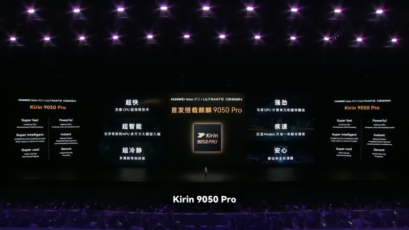
The Kirin 9050 Pro, revealed at a flagship event alongside the Mate XT 2 tri-fold launch, is the first commercial chip built on the LogicFolding architecture — a 3D-stacking approach that achieves transistor density gains by reorganizing silicon vertically within a single die rather than by shrinking transistors to smaller sizes. That distinction matters strategically: shrinking transistors requires increasingly advanced lithography equipment, and Huawei's access to the most advanced such equipment — ASML's extreme ultraviolet machines — has been blocked by US export controls since 2019. LogicFolding is the company's architectural answer to that constraint. Whether the answer holds at commercial scale is what the next several months will determine.
The Kirin 9050 Pro also represents validation — or failure — of something larger than a single chip. It is the first real-world test of whether a Chinese-built semiconductor design ecosystem can function end-to-end without Western tools: a prototype EDA program from Peking University's School of Integrated Circuits, Empyrean Technology's domestic verification platform, and SMIC's 7nm-class manufacturing process all working in sequence. If the chip reaches mass production with the claimed specifications intact, that is evidence the sovereign stack can work. If yield problems emerge or the density figures cannot be replicated independently, it is evidence they cannot.
How LogicFolding Actually Works Inside the Kirin 9050 Pro
LogicFolding differs from the chiplet packaging that Apple, Qualcomm, and MediaTek use in a specific and meaningful way. Chiplet architectures bond separately manufactured dies together into one package — each die designed in two dimensions, then combined. LogicFolding, by contrast, keeps everything within a single monolithic die and reorganizes the spatial layout of the logic itself, as the Peking University prototype EDA tool is specifically designed to support.
The current implementation stacks two silicon wafers face-to-face using hybrid bonding face-to-face wafer technology, creating ultra-high-density vertical interconnections between layers. Through-silicon vias then route signals, power, and ground outward from the bottom wafer's backside. The result is a chip in which signals travel up and down between layers along short vertical paths rather than taking longer horizontal routes across the chip surface — reducing resistive and capacitive loads in the process.
This is not a packaging trick. It is a redesign of how the logic is laid out in the first place. Peking University's prototype EDA tool supports this by treating the entire multilayer chip as one unified three-dimensional design space from the start, rather than designing each layer in two dimensions and stacking them afterward. Early tests on open-source circuit designs using that tool showed a 30% wire-length reduction measured in total internal wire length compared with conventional EDA workflows, along with improvements in performance and thermal behavior.
Huawei's engineers described the signal path as an "elevator" inside the chip, with logic moving vertically rather than horizontally. The Tau Scaling Law ISCAS keynote that underpins the approach proposes replacing Moore's Law's transistor-count metric with a different optimization target: minimizing τ (tau), the signal-travel time across every layer of the system. By that metric, LogicFolding makes progress not by building smaller transistors but by making their signals move faster — a path that does not require the extreme ultraviolet lithography machines Huawei cannot obtain.
What the Kirin 9050 Pro's Silicon Actually Contains
The chip Huawei shipped on Monday carries the following architecture, as stated at launch and corroborated by independent hardware coverage:
The LinxiCore CPU uses a nine-core, four-cluster configuration: one ultra-large core for peak single-threaded work, two performance cores for demanding tasks, four high-efficiency large cores for sustained multi-threaded loads, and two small cores handling background processes. That granular structure is designed to give the operating system's scheduler finer control over power and thermal headroom than a conventional big-little arrangement allows. Huawei claims a 24% improvement in single-core speed and 52% in multi-core throughput versus the Kirin 9030 Pro, with an overall device performance gain of 42% versus the previous Mate XT. All of these are Huawei-stated figures. Peak frequency is 3.1 GHz — the same target He Tingbo announced at the IEEE International Symposium on Circuits and Systems in May 2026 when LogicFolding was first presented to the industry, as confirmed in the He Tingbo July engineering paper.
A pre-launch leaked Geekbench 6 single-core score of 2,084, attributed to the chip by Chinese tech tipster Digital Chat Station and reported by Remio.ai, offers a partial independent data point — though its attribution to the Kirin 9050 Pro specifically remains an inference rather than a confirmed result. For context: Apple's A18 Pro scores approximately 3,582 in Geekbench 6 single-core, and Qualcomm's Snapdragon 8 Elite (2024) scores approximately 3,155, according to the A18 Pro vs Snapdragon comparison. The Kirin 9050 Pro, even accepting the leaked figure at face value, trails both by a significant margin in raw single-core output.
The Maleoon GPU adds hardware ray tracing to a Kirin mobile chip for the first time. Huawei claims a 142% improvement in graphics rendering performance versus the Kirin 9030 Pro — a Huawei-to-Huawei comparison that does not establish competitiveness with Qualcomm's Adreno 800-series or Apple's GPU, both of which have offered hardware ray tracing for several generations. Coverage confirmed hardware ray tracing Maleoon GPU at launch.
The Da Vinci NPU has been scaled to handle on-device inference for Mixture-of-Experts models with up to 30 billion total parameters, with 2 billion active at a time, as confirmed in Da Vinci NPU MoE capacity reporting. The MoE architecture, common in recent large language models including early Mistral and Google Gemini variants, activates only a fraction of total parameters for any given input — making larger total model capacity economically viable for on-device inference. This puts the chip's AI specification in direct competition with Apple's Neural Engine claims expected to be announced at the forthcoming iPhone event, though comparing on-device AI performance across architectures requires independent testing neither company has yet provided.
EAL5+ security certification with post-quantum cryptographic algorithms baked into hardware addresses growing concern that current asymmetric encryption schemes will eventually be broken by quantum computers. NIST post-quantum cryptography standards 2024 were finalized in August of that year. For users outside China — which currently means essentially no one, given the Mate XT 2's China-only launch — the practical relevance of EAL5+ certification from Chinese evaluators rather than Western security bodies is a separate question.
The Balong modem supports Tiantong satellite calling and BeiDou satellite messaging, with Huawei claiming 42% improvement in air-interface throughput and seamless satellite/cellular switching, according to confirmed Balong modem satellite connectivity coverage. A graphene-enhanced vapor chamber is said to reduce gaming temperature rise by 2.5°C (4.5°F) compared with the previous generation.
The Gap Between the Chip and the Roadmap
The Kirin 9050 Pro's transistor density claim — 55% more than the Kirin 9030 Pro, rising from 155 million to 238 MTr/mm² density claimed — is significant if it holds independently. It remains unverified. At 238 MTr/mm², the chip would approach the density range of TSMC's 3nm process, but through architectural stacking rather than lithographic scaling. Huawei has framed these as comparable; no independent party has tested whether performance, power efficiency, and yield at that density level match what TSMC's 3nm achieves in production.
The EDA constraint is the roadmap's most consequential unresolved problem. Peking University's prototype tool demonstrated 30% wire-length reductions in open-source circuit tests — but open-source circuit testing is not commercial production. The Peking University prototype EDA tool requires years of development, extensive process design kit integration with foundries, and validation across thousands of tape-outs before it is suitable for commercial use, according to Tom's Hardware. No commercial EDA software from Synopsys, Cadence, or Siemens EDA has been adapted for LogicFolding's vertical integration methodology. Huawei's own access to US EDA tools has been under export licensing scrutiny since the Bureau of Industry and Security informed design automation software suppliers in September 2025 that sales to China require a license.
Huawei itself acknowledged the manufacturing challenges in a July 2026 engineering paper by He Tingbo — the chairwoman of Huawei's Scientist Committee and president of HiSilicon — that expanded on the Tau Scaling Law: the company explicitly flagged heat dissipation and production yield as problems to be solved, and called for broader industry collaboration to develop the tools, standards, benchmarks, and manufacturing technologies the approach requires. The He Tingbo July engineering paper reads differently from inside and outside China: within China, it is an invitation to domestic EDA, foundry, and packaging partners; from outside, it is an acknowledgment that the sovereign stack is not yet complete.
Huawei's roadmap projects transistor density equivalent to a 1.4nm process by 2031 by adding more vertical layers — three-tier, four-tier, and eventually multi-tier stacking, as detailed in the He Tingbo July engineering paper. TSMC plans to begin volume production of actual 1.4nm chips in 2028 — three years earlier than Huawei's target, and using a lithography process rather than architectural approximation. The word "equivalent" in Huawei's roadmap carries significant weight: the performance, yield, and power-efficiency properties of density-equivalent chips built on older lithography have not been established by any independent party. Semiconductor analyst William Martin Keating of Semicon Alpha has noted that closing that gap will depend on whether LogicFolding can match TSMC's most advanced processes on power efficiency, yield, and manufacturing reliability — none of which has been demonstrated as of the Kirin 9050 Pro's launch.
Why Huawei Launched Monday and What the Numbers Behind It Mean
The Guangzhou event was not timed arbitrarily. Apple is expected to unveil its latest iPhone lineup this Wednesday, September 10 — what would be Apple's first foldable iPhone is widely anticipated to debut at the same presentation. Xiaomi revealed a rival tri-fold foldable device later on Monday. Huawei placed its Kirin announcement at the start of what amounts to a foldable-phone week in the global smartphone calendar.
The market position that backstops the timing is real. According to IDC data, Huawei led China smartphone market share reached 22.6% in the second quarter of 2026, ahead of Apple at 18.1% and Xiaomi at 12.4%, with year-on-year shipment growth of 19.4%. Smart Analytics Global data puts Huawei's 68% foldable market share of China's foldable-phone segment in the same period. Those are domestic numbers — the US market remains entirely closed to Huawei products, and the FCC's July 2026 Open Commission Meeting formalized the ban on new devices containing Huawei chips entering the American market.
The financial infrastructure behind the chip is substantial. Huawei's record R&D spending first half of 2026 reached ¥121.38 billion (approximately $17.9 billion USD), a record for the period and more than a quarter of total revenue — a figure confirmed by Xinhua citing Huawei's own data. That level of sustained R&D investment, maintained across six years of constrained manufacturing access, is what made a project of LogicFolding's complexity possible. The Kirin 9050 Pro is, in one reading, the commercial proof-of-concept for that investment — the delivered product that either validates or exposes the roadmap.
The Mate XT 2 pricing sales date will go on sale in China beginning September 12, with pricing from ¥19,999 (approximately $2,980 USD) to ¥24,999 (approximately $3,725 USD). Richard Yu, Huawei's consumer business chief, acknowledged at the press conference that rising memory prices and the cost of integrating new technology made the device genuinely challenging to price.
What This Chip Costs Buyers Outside China
The Mate XT 2 is launching exclusively in China. But the legal framework that applies to Huawei hardware does not respect geography.
China's National Intelligence Law of 2017, Article 7, requires all Chinese organizations and citizens to support, assist, and cooperate with national intelligence work in accordance with the law. Article 14 grants Chinese intelligence agencies the authority to demand that cooperation from any organization or individual. These obligations apply to Huawei regardless of where its devices are manufactured, where their servers are located, or what Huawei's privacy policy states. The US Federal Communications Commission cited the National Intelligence Law by name in its June 2020 order — FCC 2020 covered company order (DA-20-690) — designating Huawei a covered company under national security rules, finding that the law compels Huawei to assist the Chinese government in espionage activities. Supplementing it: China's Cybersecurity Law (2017) and Data Security Law (2021) add data localization requirements and mandatory government access provisions.
No backdoor has been confirmed in the Kirin 9050 Pro specifically. The legal obligation for cooperation with Chinese state intelligence exists regardless.
Data that a Mate XT 2 running HarmonyOS 7 could collect and that would be subject to these legal demands includes location data, call metadata, biometric data used for authentication, device usage patterns, documents processed on-device, and network activity. Categories of sensitive data depend on which apps are installed and what permissions are granted — but the legal framework applies to the operating system level regardless of app configuration.
The National Bureau of Asian Research's analysis of the National Intelligence Law concludes that "the CCP almost certainly could compel Huawei to provide customer data or network access upon request," and that Huawei's founder Ren Zhengfei's stated willingness to refuse such a request would be, in the view of legal experts, legally impossible to act on. A 2025 Tandfonline academic analysis of Huawei's UK corporate structure reached the same conclusion about the law's extraterritorial reach.
For enterprise buyers in regulated industries outside China who encounter Huawei hardware — through subsidiary offices, supply chain, or regional procurement — the practical mitigation options are limited: network segmentation can restrict device-level data transmission but cannot prevent on-device collection by the operating system itself. No VPN or software control fully addresses the structural legal risk. The cleanest mitigation remains not deploying the hardware in environments that handle sensitive data.
What Comes Next for LogicFolding
The semiconductor industry's immediate question is whether the Kirin 9050 Pro's commercial launch produces independently verifiable numbers. If it does — if a teardown analysis confirms the 238 MTr/mm² density figure, and if sustained benchmark testing confirms competitive energy efficiency — then LogicFolding's architectural logic will demand attention far beyond China's domestic market. A credible path to 3nm-class performance density without EUV lithography would reshape assumptions about what chip design can accomplish under geopolitical constraint.
If independent testing reveals significant gaps between the launch claims and real-world performance — in yield, in sustained performance under thermal load, or in energy efficiency relative to Apple and Qualcomm — then the Kirin 9050 Pro will be recorded as a sophisticated proof-of-concept that did not close the manufacturing gap it was designed to close.
The EDA tooling timeline is the factor least visible to outside analysts but most consequential to the roadmap. Empyrean's Argus platform and Peking University's prototype tool represent the beginning of a domestic EDA ecosystem, not its completion. Bringing a research prototype to production-grade validation — with full process design kit integration, regression testing across commercial circuit libraries, and thousands of tape-out validations — is measured in years, not months. How quickly that maturation happens will determine whether the Kirin 9050 Pro remains a singular achievement or becomes the first chip in a scalable roadmap.
Read more: Huawei LogicFolding Chip Claims 54% Density Gain: No Independent Audit Yet
The 2031 density roadmap, the 4 GHz frequency target, the multi-tier stacking progression — all of those depend on solving heat dissipation, production yield, and EDA tooling challenges that Huawei's own engineers have acknowledged in print. Closing a five-year manufacturing gap with TSMC through architecture rather than process chemistry is the most ambitious claim in the Tau Scaling Law. Monday's launch is the moment that claim moved from a preprint to a product. The verification of whether the product delivers on the claim is still ahead.
Read more: Huawei Unveils Kirin X90 Plus and XE90: China's PC Chip Push Hits SMIC's 7nm Ceiling
Exchange rate as of September 7, 2026; conversions are approximate.
Frequently Asked Questions
How does LogicFolding differ from the chiplet packaging used in Apple and Qualcomm chips?
Chiplet packaging bonds separately manufactured dies together into a single package — each die is designed in two dimensions, then physically joined to others. LogicFolding keeps everything within a single monolithic die but reorganizes its layout in three dimensions, stacking active silicon layers face-to-face using hybrid bonding and connecting them with through-silicon vias. The critical distinction is the EDA tooling: Peking University's prototype tool treats the entire multilayer structure as one unified vertical design space from the beginning of the design process, rather than designing separate 2D layers and stacking them afterward. In early tests on open-source circuits, this approach reduced total internal wire length by 30%. Whether that prototype tool scales to commercial production validation — requiring thousands of tape-outs and full process design kit integration — is the central open question the Kirin 9050 Pro's commercial launch has not yet answered.
Is the Kirin 9050 Pro's performance competitive with Apple's A18 Pro or Qualcomm's Snapdragon 8 Elite?
Not in raw single-core output, based on available pre-launch data. A leaked Geekbench 6 single-core score attributed to the Kirin 9050 Pro by Chinese tipsters puts it around 2,084 at 3.1 GHz — a 12% improvement over the Kirin 9030 Pro, but well below Apple's A18 Pro (approximately 3,582) and Qualcomm's Snapdragon 8 Elite (approximately 3,155). The 42% overall performance improvement Huawei claims is a comparison against the previous Mate XT, not against Apple or Qualcomm devices. No independent benchmark organization had verified any Kirin 9050 Pro performance figure at the time of this writing. The claim that the chip's performance is "comparable to TSMC's 3nm" comes from Huawei and Huawei-aligned media, and has not been confirmed by an independent third party. Independent testing when review units become available will determine whether the performance gap narrows meaningfully.
What does China's National Intelligence Law mean for anyone who acquires a Mate XT 2 — now or in the future?
China's National Intelligence Law of 2017, Articles 7 and 14, require all Chinese organizations to support and cooperate with intelligence work on demand, with no geographic limitation on that obligation. The law applies to Huawei regardless of where a device's servers are physically located, regardless of Huawei's stated privacy policies, and regardless of the legal structure of any Western subsidiary. The US Federal Communications Commission cited this law by name in its 2020 order designating Huawei a covered national security threat. For any buyer who acquires a Mate XT 2 outside of China — should international availability follow — the legal framework is a fixed structural condition, not a contingent risk. No backdoor has been confirmed in the Kirin 9050 Pro specifically, but the legal obligation for Huawei to cooperate with Chinese state intelligence upon government request applies regardless of chip architecture.
Why has no independent auditor verified the LogicFolding density claims four months after the architecture was announced?
The timeline between architectural announcement and independent verification for a novel chip design is typically measured in quarters, not weeks. Verifying transistor density at 238 million transistors per square millimeter requires physical teardown analysis — the kind of work that firms like TechInsights and SemiAnalysis perform, which involves decapping the chip, performing electron microscopy, and comparing measurements to published specifications. As of this writing, the Kirin 9050 Pro has been publicly available for hours. Independent density verification will require access to retail units, lab time, and comparison against the specific process node used at SMIC — whose N+3 node was itself only independently analyzed for the first time in June 2026. The absence of independent verification is not evidence of falsification; it is a function of the timeline. The verification will come. What it shows will determine whether LogicFolding's claims are the beginning of a new chapter in mobile chip design or a carefully staged performance.

-
 C114 Communication Network
 -
 Communication Home
