
 Search

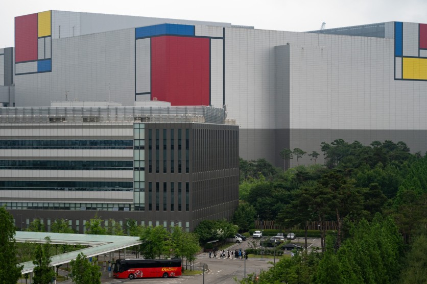
A general view shows buildings at the Samsung Electronics factory in Pyeongtaek on May 28, 2026. Shin Yong-ju/gettyimages.com
Samsung Electronics' next-generation megafab at Pyeongtaek has crossed a milestone that turns a production promise into a physical reality. Hanyang ENG, a specialized Korean engineering contractor, disclosed in a regulatory filing on September 7 that it had signed a ₩148.06 billion ($110 million) contract with Samsung C&T to install the first general piping zone for the Phase 1 cleanroom at Samsung's Pyeongtaek P5 facility. The contract, worth 13.24% of annual revenue, runs through September 30, 2027, and will be funded with a 10% advance payment within 15 days of signing, with the remaining 90% paid in progress-based installments as Samsung C&T verifies completed work.
The filing matters because of what it confirms: Samsung P5's Phase 1 cleanroom is no longer a planning document. Construction crews are actively building the utility infrastructure — the arterial network of pipes that will carry ultrapure water, industrial chemicals, process gases, and cooling water to every semiconductor manufacturing tool on the production floor.
"General piping involves installing piping networks that safely supply and discharge ultrapure water, chemicals, industrial gases and cooling water used in semiconductor manufacturing to and from equipment on each production line," a Hanyang ENG official said. "The first work zone refers to the primary main piping."
Read more: TSMC Equipment Demand Doubled, But Fab Construction Workers Are Running Out
Why Piping Has to Come First
The sequencing rule that makes this contract significant is one most observers of the semiconductor supply chain overlook: cleanroom process piping must be installed, flushed, tested, and certified before a single piece of semiconductor manufacturing equipment can be delivered to the facility. The industry calls this milestone "Readiness for Equipment," or RFE — a formal checkpoint at which the cleanroom is certified as ready to accept tools. Until piping reaches RFE, there is no floor for tools to sit on in any functional sense.
This means the 8–10 month main piping timeline is not just a construction milestone — it is the leading indicator for the entire P5 production ramp. Equipment orders, delivery logistics, and installation scheduling all flow from when piping achieves RFE. "The actual main piping work will be largely completed in about eight to 10 months," the Hanyang ENG official said, adding that the contract value may be revised if the scale of facilities changes or additional work is required.
A facility like P5, which Samsung has described as a future hub for high-bandwidth memory production, consumes resources at a scale that requires an equally massive utility infrastructure. Advanced semiconductor fabs consume 2–4 million gallons of ultrapure water per day — water purified to resistivity specifications far beyond pharmaceutical-grade standards, distributed through electropolished stainless steel piping that must remain free of contamination throughout installation.
Hanyang ENG's scope extends beyond water. The "general piping" contract also covers Chemical Central Supply System infrastructure — the centralized network that safely stores, monitors, and distributes hazardous process chemicals including hydrofluoric acid and phosphoric acid to individual tool stations. Hanyang ENG is notable for domesticating CCSS technology for Korean fabs, earning a Bronze Tower Order of Industrial Service Merit — meaning it was the first Korean company to develop this capability domestically rather than importing it from foreign suppliers.
What P5 Is and Why Its Timeline Matters
P5 is Samsung's largest planned semiconductor facility at Pyeongtaek — and by most measures, the largest planned semiconductor facility in the world. The building measures 650 meters wide and 195 meters long, organized across three floors with six cleanrooms, compared with four cleanrooms across two floors at earlier P1-P4 plants. The total investment across the P5 facility is estimated at $23 to $46 billion depending on the product mix and equipment density ultimately deployed.
Samsung has positioned P5 as a future production hub for HBM — the high-bandwidth memory that every Nvidia AI accelerator requires, and for which global supply has remained severely constrained through 2026. Samsung recently reclaimed its position as the world's largest DRAM supplier, and its HBM4 yield has been improving steadily. P5 Phase 1 equipment installation beginning in earnest after mid-2027 would represent one of the largest single additions to global HBM production capacity in the history of the industry.
Read more: Samsung Weighs Shipping Legacy Memory Backend to Vietnam to Unlock HBM Capacity
Acceleration and the Shell First Strategy
The Hanyang ENG contract is the product of deliberate schedule compression. In February 2026, Samsung sent construction partners a request to advance the cleanroom build-out schedule by roughly six months compared to earlier plans as part of its "six-month cleanroom acceleration plan" — consistent with its "Shell First" strategy of completing building structure and utility infrastructure ahead of market demand, enabling rapid equipment deployment when conditions justify it.
Under the original schedule, full-scale cleanroom construction was not expected to begin until early 2027, with piping installation targeted for the same year. Under the accelerated plan, preparatory works moved to Q2 2026, cleanroom build-out began in early Q3 2026 (July), and piping installation — confirmed by the September 7 Hanyang ENG filing — is now under signed contract and active execution. "Cranes deployed at P5 site — the construction site is very busy," an industry insider told SammyGuru in February 2026.
Hanyang ENG is not the only contractor operating at P5. Samsung C&T is coordinating parallel work streams across multiple specialized subcontractors: Shinseong ENG received a ₩15.6 billion contract to supply cleanroom equipment, and Exy&C received an ₩89 billion contract for interior finishing work at Phase 1 of the facility. This parallel contracting model compresses the overall construction timeline by eliminating sequential handoffs between major work packages.
The approach reflects both the scale of demand and the scarcity of the specialized workforce that can execute it. As former ASML CEO Peter Wennink noted in TechTimes coverage just days earlier, the skill required to build semiconductor fabs has been refined over decades in only a few places on the planet — predominantly in Taiwan and South Korea. Hanyang ENG, founded in 1988, represents exactly that deep institutional knowledge.
The Path From Pipe to Production
The construction sequencing from today's piping contract to Samsung's stated late-2028 mass production target runs through a set of milestones that are now backed by signed contracts and active field crews. Main piping is expected to be substantially complete in 8–10 months — roughly May through July 2027. The Hanyang ENG contract itself runs through September 30, 2027, providing buffer for any scope additions.
Industry analysts report that construction is complete by mid-2027 per analysts, at which point equipment installation can begin in earnest. Samsung is reportedly bringing in tens of thousands of workers to construct the megafab. Mass production carries a late-2028 mass production target that the accelerated construction schedule is designed to protect. Separately, Samsung is also advancing P5 Fab 2 — originally planned as a standalone facility, now being designed to connect directly to P5 in a "Fab Twin" configuration.
Hanyang ENG, for its part, has signed similar contracts with Samsung C&T every year for the past three years, underscoring both the continuity of the relationship and the scale of ongoing Samsung capital investment at Pyeongtaek. The company posted H1 2026 revenue of ₩696.06 billion, with operating profit of ₩50.8 billion and net profit of ₩47.89 billion — numbers that reflect the sustained demand for specialized cleanroom and piping services as South Korea's semiconductor industry executes some of the most capital-intensive construction projects in human history.
Frequently Asked Questions
When will Samsung's P5 fab start making chips?
Samsung is targeting mass production at P5 Phase 1 in the latter part of 2028. Under the current accelerated construction schedule, the Phase 1 cleanroom structure is expected to be substantially complete in the first half of 2027. Equipment installation would then begin, followed by process qualification and ramp. The Hanyang ENG piping contract — with an 8–10 month main piping timeline — is the milestone that must be reached before equipment installation can begin in earnest.
What is ultrapure water and why does a chip factory need so much of it?
Ultrapure water is water purified to resistivity levels far exceeding pharmaceutical standards — so pure it is essentially an electrical insulator. Semiconductor fabs use it to rinse wafers between manufacturing steps, removing chemical residues without introducing contamination. A large modern fab consumes 2–4 million gallons of ultrapure water per day. The piping network that distributes this water throughout the facility must be installed and certified before any manufacturing tools arrive, which is why cleanroom piping is the gating milestone in fab construction sequencing.
What is a Chemical Central Supply System (CCSS) and why does it matter?
A Chemical Central Supply System is the centralized infrastructure that safely stores, mixes, monitors, and distributes the hazardous process chemicals used in semiconductor manufacturing — hydrofluoric acid, phosphoric acid, ammonium hydroxide, and others — to individual tool stations throughout the cleanroom via dedicated piping networks. CCSS installations include leak detection, secondary containment, gas detection, and automated emergency shutoff systems. Hanyang ENG was the first Korean company to domesticate this technology, reducing South Korea's dependence on foreign suppliers for a safety-critical component of every semiconductor fab.
What does Samsung's P5 facility mean for AI chip supply?
High-bandwidth memory, or HBM, is the memory technology inside every high-performance AI accelerator. Samsung's P5, when operational, would represent one of the largest single additions to global HBM production capacity in the industry's history. P5 has six cleanrooms across three floors — roughly equivalent to combining Samsung's P3 and P4 facilities — and is projected to require a total investment of $23 to $46 billion. Every Nvidia AI GPU requires HBM; P5 coming online in late 2028 is expected to provide meaningful relief to the AI memory supply crunch that has constrained AI infrastructure buildout since 2024.
What is Samsung's Shell First strategy?
Shell First is Samsung's approach to large-scale fab construction in which the building shell and utility infrastructure — cleanroom space, piping, power substations, HVAC — are completed ahead of specific equipment decisions and market demand signals. This allows Samsung to rapidly deploy manufacturing equipment once demand conditions justify it, without waiting for the longer lead times associated with building construction itself. The Hanyang ENG piping contract is a direct output of this strategy: Samsung accelerated the piping installation schedule by roughly six months in early 2026, and the signed contract confirms that acceleration is backed by committed capital and active fieldwork.

-
 C114 Communication Network
 -
 Communication Home
