

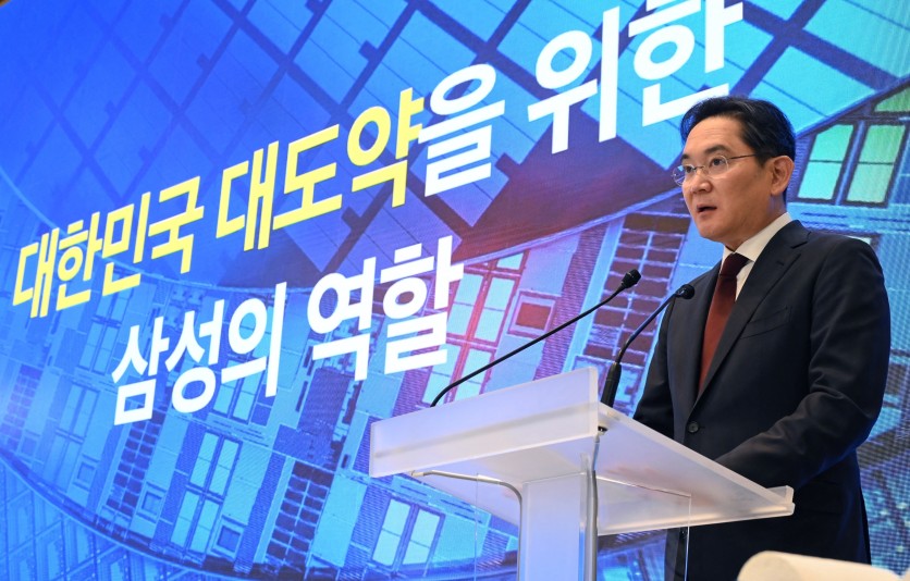
Samsung Electronics Chairman Lee Jae-yong attends the briefing announcement of public-private collaboration projects at the presidential Blue House in Seoul on June 29, 2026. South Korea will invest nearly $1.2 trillion -- equivalent to more than two-thirds of its GDP -- in a new chip-building hub and AI data centres over several years, as it seeks to profit from soaring demand while developing previously neglected regions. KIM Min-Hee/AFP via Getty Images
Samsung Chairman Lee Jae-yong fleshed out the company's role in Korea's June 29 mega-project, naming Gwangju as the candidate site for a new semiconductor complex, the Chungcheong region for HBM packaging, and Gumi for robotics — part of a group-wide push spanning chips, batteries, bio, and shipbuilding.
Read closely, the announcement is less a spending figure than a map. Lee did not just say Samsung would invest heavily; he said where each bet would land and why — and the logic of those placements is a small window into how the AI era is reshaping Korea's industrial geography.
"Speed Battle": Why a New Complex, and Why Now
At the national briefing held at the former Blue House, Lee said the AI technology paradigm is shifting at "unimaginable speed" and demand is outstripping even aggressive investment, prompting Samsung to accelerate its Yongin and Pyeongtaek timelines and move up plans for a new complex. Calling it a "speed battle," he framed the new sites as a response to demand arriving faster than existing hubs can be filled.
Gwangju: Chosen for Power, Water, and an Existing Back-End Ecosystem
Lee pointed to Gwangju — where power, water, workforce, and infrastructure incentives are expected, and where a back-end ecosystem including outsourced assembly and test (OSAT) firms such as Amkor already exists — as the leading candidate, with sites reportedly under review in Gwangju's Cheomdan 3rd District and the Bitgreen industrial complex.
The choice illustrates the trade-offs in placing a fab. Chip-making divides into front-end work (etching circuits onto wafers, the most demanding step) and back-end work (cutting, stacking, and packaging the finished chips). Gwangju offers ample power, water, and land plus an established back-end testing-and-packaging ecosystem — but, as industry analysts note, it lacks the deep front-end supplier base and specialized workforce that a region like Yongin has built up, which is part of why Samsung still describes it as a leading candidate rather than a settled choice.
Read more: South Korea Unveils $649B Samsung-Led AI Push Into Chips, Data Centers, Robots
Chungcheong: Where Packaging Became as Hard as the Main Fab
For advanced packaging, Lee said HBM — indispensable for training and running AI models — demands main-fab-level process difficulty, and Samsung would concentrate its HBM fabs alongside its existing back-end fabs in Cheonan and Onyang in the Chungcheong region.
That single line carries a real shift. For most of the industry's history, packaging was the comparatively easy part of making a chip. HBM has upended that: because it works by stacking many DRAM dies into a single tower and wiring them together with extreme precision, the packaging step has become nearly as difficult as etching the wafer itself. Concentrating HBM fabs where the back-end expertise, equipment, and ecosystem already live — Cheonan and Onyang — follows the same logic that points the new front-end complex toward an existing ecosystem in Gwangju.
Read more: Samsung Quantifies Hybrid-Bonding's Edge in Cooling Next-Gen HBM
The Rest of the Map: Robots, Substrates, Batteries, Ships, Bio
Lee detailed affiliate plans by region, and each follows the same principle of matching a business to where its inputs and infrastructure cluster. Physical AI, humanoid robotics, and internal-use AI data centers will center on Gumi, with robot demand expected to grow across factories, homes, restaurants, hospitals, and care facilities. Samsung Electro-Mechanics will expand server FC-BGA substrate capacity in Sejong and Busan to meet North American big-tech demand for AI servers.
Samsung SDI will focus next-generation all-solid-state batteries and energy-storage (ESS) cells on Ulsan, while developing its Cheonan plant — its small-battery hub, where dry-electrode technology is in development — into a global "mother factory." Samsung Heavy Industries will base next-generation shipbuilding in Geoje, and Samsung Biologics will concentrate investment in Songdo to build what it calls the world's largest bio complex.
The Doctrine: "Overwhelming Gap"
Tying it together is the competitive philosophy Lee returned to at the end. Maintaining "a sense of crisis," he said, Samsung would pursue customer focus, quality, technological innovation, and talent to lead with an "overwhelming gap" — cho-gyeokcha — over rivals: the belief that Samsung wins not by matching competitors but by opening a lead too large to close. Placing each bet where the infrastructure, ecosystem, and government support already align is, in that framing, how the gap gets built.
All of these remain announced plans and candidate sites, stretching over roughly a decade, and subject to demand, infrastructure, and final site selection. Samsung's shares fell on the day of the announcement, a reminder that investors are still weighing the scale of the spending against the returns. But as a statement of intent, Lee's map lays out not just how much Samsung will invest, but the reasoning for where.
Frequently Asked Questions
Where will Samsung build its new chip plant?
At Korea's June 29 mega-project briefing, Samsung Chairman Lee Jae-yong named Gwangju as the leading candidate site for a new semiconductor complex, citing expected support for power, water, workforce, and infrastructure, along with an existing back-end ecosystem that includes OSAT firms such as Amkor. Specific locations reportedly under review include Gwangju's Cheomdan 3rd District and the Bitgreen industrial complex. Lee described Gwangju as a candidate rather than a finalized choice, in part because the region lacks the deep front-end supplier base of established hubs like Yongin.
Why is Samsung putting HBM packaging in Chungcheong?
Lee said high-bandwidth memory (HBM), which is essential for training and running AI models, now requires "main-fab-level" process difficulty because it involves stacking many memory dies and wiring them together with extreme precision. Because that advanced packaging has become nearly as demanding as front-end chipmaking, Samsung plans to concentrate its HBM fabs alongside its existing back-end fabs in Cheonan and Onyang, in the Chungcheong region, where the relevant expertise, equipment, and ecosystem already exist.
What is Samsung building in Gumi?
According to Lee, Samsung will center its physical AI, humanoid robotics, and internal-use AI data center efforts in Gumi, in North Gyeongsang province. Lee said robot demand is expected to grow not only in factories and industrial settings but across homes, restaurants, hospitals, and care facilities, positioning robotics as a major future business for the group as part of its broader AI strategy.
What is Cho-gyeokcha?
Cho-gyeokcha is a Korean term often translated as "overwhelming gap" or "super gap." It refers to Samsung's long-standing competitive doctrine of trying to lead rivals by a margin so large that competitors cannot easily catch up, rather than competing on incremental improvements. At the June 29 briefing, Lee invoked the concept while saying Samsung would maintain "a sense of crisis" and focus on customers, quality, technological innovation, and talent to stay ahead in global competition.
-
 C114 Communication Network
 -
 Communication Home
