

Through-Glass Via (TGV) Glass Substrate JNTC website
JNTC, a South Korean advanced-materials company, said on June 19 that it has developed a through-glass-via (TGV) substrate 2.0 millimeters thick — which it bills as an industry first — giving it TGV technology across a thickness range from 0.3mm to 2mm.
A note on framing: nearly everything below is JNTC's own account of its progress, announced by the company and not yet independently benchmarked. The claim is notable, but it is a milestone in development and verification, not yet mass production for a named customer.
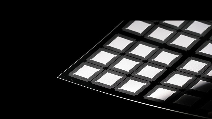
What a TGV Glass Substrate Is, and Why Thickness Is Hard
A substrate is the base a chip sits on and routes its signals and power through. A through-glass via is a microscopic vertical channel drilled and metal-filled through a glass sheet — the glass analog of the through-silicon via — letting signals pass straight through the substrate to connect chips placed around or atop it. Glass appeals because it is exceptionally flat and thermally stable, so a large AI package warps and overheats less than it would on a plastic, or organic, core.
The catch is processing. Drilling thousands of ultra-fine holes through brittle glass without spawning micro-cracks — flaws that later fail under thermal and mechanical stress — is the field's central reliability problem, and it gets harder as the glass gets thicker, because each hole must be deeper and higher in aspect ratio. That is the context for JNTC's claim: industry development has mostly centered on glass around 0.8mm to 1.0mm thick, so a defect-free part at 2.0mm, if it holds up in customers' hands, sits at the difficult end of the curve. Glass that is too thin can warp or break during packaging; glass that is too thick is harder to laser-drill and etch — which is why a wide, validated thickness range is the thing JNTC is selling.
According to the company, the 2.0mm product has passed reliability verification on glass micro-cracks with substrate makers in Taiwan and South Korea — earning what it calls a crack-free assessment — while verification continues with a maker in Japan. JNTC says it is also developing a 3mm version, aiming to finish within the year, and that it has secured the unit-cell-cut processing some customers have requested.
Read more: TSMC Readies Panel-Level Packaging for AI Chips, Setting Up a Showdown With Samsung
The Cheaper-Build Angle
Glass substrates are drawing intense interest as a successor to today's organic substrates for AI and high-performance-computing chips, and the field is crowded — TSMC, Intel, Samsung, Japan's Rapidus, and SK's U.S. unit Absolics are all chasing it. JNTC's claimed edge is partly cost. To build out the operation after entering the business in 2024, it absorbed its plating-and-etching subsidiary Comet last year, used equipment self-built by affiliate Jinwoo Engineering to improve quality and cost, and completed a domestic TGV mass-production line in October — vertically integrating its front-end processes. That in-house-equipment approach, the company has said, cut its initial investment to roughly a fifth of the industry norm. JNTC says it is now working on new projects with two of the world's largest comprehensive semiconductor companies, though it does not name them.
A Materials Maker Pivoting to AI
JNTC is targeting mass production by 2027, with projects and evaluations underway. In May it signed a memorandum of understanding with a major Korean conglomerate, and it says an additional contract with a Japan-based global substrate maker is due next month. CEO Andrew Cho (Cho Nam-hyeok) called the TGV glass-substrate business a critical medium-to-long-term growth pillar — part of the company's broader pivot from a mobile-IT cover-glass supplier, a business it describes as having become a price-only market, toward an AI-focused one. Investors reacted sharply to the announcement, sending JNTC's KOSDAQ-listed shares to their daily upper limit.
Whether the thickness milestone translates into real revenue still depends on the part that no press release can settle: qualification and high-volume yield in a named customer's packaging line. The technology claim is JNTC's to make; the verdict belongs to the chipmakers it is courting, and on the company's own timeline that verdict lands around 2027.
Frequently Asked Questions
What is a through-glass via (TGV)?
A through-glass via is a tiny vertical electrical channel drilled through a glass substrate and filled with metal, allowing signals and power to pass straight through the glass to connect chips placed around or on top of it. It is the glass counterpart to the through-silicon via used in chip stacking, and it is a core building block of glass-based advanced packaging for AI processors.
Why are glass substrates better for AI chips?
Glass substrates are prized for flatness and thermal stability, which reduce the warpage and heat buildup that large, high-power AI packages suffer on conventional plastic (organic) substrates. That can improve power efficiency and signal integrity, which is why glass is widely seen as the next frontier in advanced packaging — though the technology is still moving from development toward volume manufacturing across the industry.
What did JNTC actually announce?
JNTC said it developed a TGV glass substrate 2.0 millimeters thick, which it calls an industry first, giving it a lineup spanning 0.3mm to 2.0mm. It said the product passed micro-crack reliability checks with substrate makers in Taiwan and South Korea, with a Japanese maker's verification ongoing, and that it is developing a 3mm version. These are the company's own claims, and it is targeting mass production by 2027.
Why does the thickness of a glass substrate matter?
Thickness sits at the heart of glass-substrate manufacturing difficulty. Too thin, and the glass can warp or break during packaging; too thick, and it becomes harder to laser-drill and etch the via holes without creating micro-cracks. Most industry development has centered on glass roughly 0.8mm to 1.0mm thick, so JNTC's claim of a defect-free 2.0mm part — and a full 0.3mm-to-2.0mm range — is meant to signal a processing-capability edge.
-
 C114 Communication Network
 -
 Communication Home
