

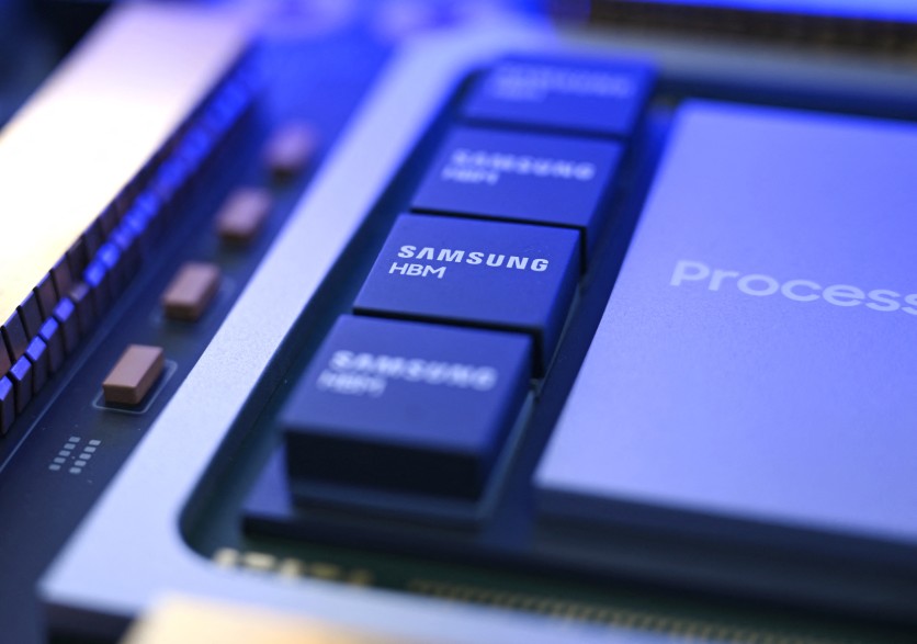
This picture taken on October 22, 2025 shows a mockup of a chipset featuring Samsung Electronics' high-bandwidth memory (HBM) technology on display during the 2025 Semiconductor Exhibition in Seoul. South Korean tech giant Samsung Electronics said on February 12, 2026 it has started mass production of a next-generation memory chip to power artificial intelligence. Jung Yeon-je/AFP via Getty Images
Samsung Electronics unveiled the world's first physical mock-up of its eighth-generation high-bandwidth memory, HBM5, at Computex 2026 in Taipei on Tuesday, June 2, introducing a new thermal architecture called Heat Path Block and confirming plans to build the product's base die on a 2-nanometer process. The announcement signals Samsung's intent to lead the next wave of AI memory competition — but at the same Computex show, Nvidia CEO Jensen Huang visited the SK hynix booth the day before, wrote "Please Make More" on an HBM4E wafer, and praised the company's trillion-dollar market valuation in front of SK Group Chairman Chey Tae-won — leaving Samsung's rival to claim the week's most visible Nvidia endorsement.
Song Jae-hyuk, president and chief technology officer of Samsung's Device Solutions division, walked reporters through the HBM5 mock-up at the Samsung Display booth — Samsung's chip division did not set up its own stand, instead taking a corner of the display exhibit in a decision made roughly ten days before the show opened. Song's message was about systems-level integration: thermal management, packaging, and foundry capability are now just as important as raw memory performance. "Artificial intelligence technology is not a single technology," he said. "It is crucial to optimize the entire system, including memory, packaging, and thermal management."
How Heat Path Block Solves AI Memory Heat Between Stacked Dies
The central technical claim in Samsung's HBM5 presentation was Heat Path Block, or HPB — a thermal management structure that adds a dedicated heat-transfer path between the stacked dies in an HBM package. As HBM generations stack more dies and push higher data rates, the heat generated between layers accumulates faster than conventional packaging can dissipate it. HPB, Song explained, works like a chimney: it creates a separate conduit that routes heat away from the die interfaces, lowering thermal resistance and extending the chip's operational stability under sustained load.
Samsung says it has already verified HPB's structural integrity and packaging reliability through its HBM4E products — the seventh-generation memory whose first sample shipments began on Friday, May 29, 2026. That product delivers a stable pin speed of 14 gigabits per second, scalable to 16 Gbps, with a single-stack bandwidth of 3.6 terabytes per second. HPB is validated at the HBM4E level; Samsung plans to deploy it fully starting with HBM5.
The stakes behind the thermal work are real. In 2024, Samsung's HBM3E chips failed Nvidia's qualification tests due to heat and power consumption issues, according to three Reuters sources briefed on the problems. The failure cost Samsung a full generation of Nvidia business. HPB represents Samsung's direct engineering response to that failure, embedded in the HBM stack itself rather than addressed through external cooling.
HBM5 Gets a 2nm Base Die Upgrade Over the 4nm Used in HBM4
HBM stacks consist of DRAM dies on top and a logic base die at the bottom that handles communication with the host processor. Samsung's HBM4 and HBM4E use a 4nm in-house foundry process for that base die. For HBM5, Samsung confirmed at Computex 2026 that it plans to use a 2-nanometer process, a step intended to improve the base die's power efficiency and processing throughput.
This is not a surprise announcement — Samsung's memory development team disclosed the 2nm plan for HBM5 at Nvidia's GTC 2026 conference in March. What Tuesday's showing added was the first physical mock-up: a tangible artifact that hardware planners and Nvidia's engineering teams can now reference when building their next-generation system designs.
Why Nvidia Signed SK Hynix Wafers Instead of Samsung Ones
The competitive subtext at Computex 2026 was difficult to miss. On Monday, June 1, Huang visited the SK hynix booth, writing "Please Make More" on an HBM4E wafer and "Love SOCAMM" on an SK hynix memory module — a gesture SK Group's official communications described as reaffirming their joint commitment to AI infrastructure. At a private Korea Partner Night dinner the same evening, Huang praised SK hynix's trillion-dollar valuation in front of both companies' leadership. Samsung's Executive Vice President of Memory Business, Kim Jae-june, attended that dinner; his company's CTO would speak the following morning.
SK Group Chairman Chey Tae-won offered a candid market-structure observation from his company's own booth: only one customer — Nvidia — is currently requesting HBM4E. The remark was widely read as a direct counterpoint to Samsung's emphasis on being the first to ship HBM4E samples, because in a market shaped by a single dominant buyer, the question of who ships first matters less than the question of whom Nvidia chooses to buy from.
Industry analysts have consistently placed SK hynix as the larger Nvidia HBM supplier. TrendForce estimated before Computex that SK hynix would hold approximately 50 percent of global HBM bit output in 2026, with Samsung's share rising to around 28 percent. Ray Wang, a memory analyst at SemiAnalysis cited by CNBC, said he expects SK hynix to "maintain its lead in HBM4, while Samsung makes material progress and becomes more competitive." The market position is improving for Samsung, but it is not yet reversed.
What Does Samsung HBM5 Mean for AI Infrastructure Buyers?
For engineers specifying memory for systems beyond Nvidia's current Vera Rubin platform, Tuesday's showing matters as a planning signal rather than a procurement option. HBM5 is not yet in production, has no confirmed customer qualification timeline, and no independent benchmark data exists for its performance claims. What Samsung showed was a prototype of its architecture and a roadmap commitment. KAIST and industry research firms have projected HBM5 arriving in volume around 2028 to 2029, targeting 4 terabytes per second of bandwidth per stack — more than double today's HBM4E — and aimed at Nvidia's Feynman platform, two generations beyond Vera Rubin.
Samsung's legal exposure adds a caveat worth tracking. The US International Trade Commission is conducting an ongoing investigation into whether Samsung's HBM and DDR5 chips infringe six patents held by Netlist, following a complaint filed in September 2025. Industry observers consider an import ban unlikely given the depth of US hyperscalers' reliance on Samsung memory, and Samsung has described the investigation as a routine procedure. But it is a live proceeding that hardware planners with long sourcing cycles should monitor.
For now, Samsung's message at Computex 2026 was architectural confidence: it has a thermal solution it has tested, a process node it has committed to, and a roadmap generation it is willing to show publicly three years before it ships. Whether Nvidia's pen finds its way to a Samsung wafer at a future show is the question Samsung's DS division is still answering.
Frequently Asked Questions
What is Samsung HBM5 and when will it be available?
HBM5 is Samsung's eighth-generation high-bandwidth memory, designed for next-generation AI accelerators. Samsung unveiled the first physical mock-up at Computex 2026 on June 2, 2026, but has not announced a production timeline; industry analysts project HBM5 volume shipments arriving around 2028 to 2029.
What is Heat Path Block technology in Samsung's HBM5?
Heat Path Block, or HPB, is a thermal management structure built into the HBM package that adds a dedicated heat-transfer path between stacked memory dies, working like a chimney to route heat away from the die interfaces. Samsung validated the architecture in its HBM4E products and plans to deploy it fully starting with HBM5. SK hynix has a competing approach called iHBM that also targets thermal resistance in the HBM5 generation.
Why does Nvidia appear to prefer SK hynix over Samsung for AI memory?
SK hynix has held an estimated 50 to 62 percent share of the global HBM market and has been Nvidia's largest HBM supplier since the HBM3E generation. Samsung fell behind after its HBM3E chips failed Nvidia's heat and power qualification tests in 2024, and while it has recovered market share with HBM4 and HBM4E, analysts expect SK hynix to retain its Nvidia lead into the HBM4 generation.
What is the HBM5 2nm base die and why does it matter?
The base die is the logic layer at the bottom of an HBM stack that handles communication with the host processor. Samsung's HBM4 and HBM4E use a 4nm process for this layer; moving to a 2nm process for HBM5 is intended to improve power efficiency and processing throughput, giving AI accelerators better performance per watt at the memory interface.
-
 C114 Communication Network
 -
 Communication Home
