
 Search

Cxmt.com
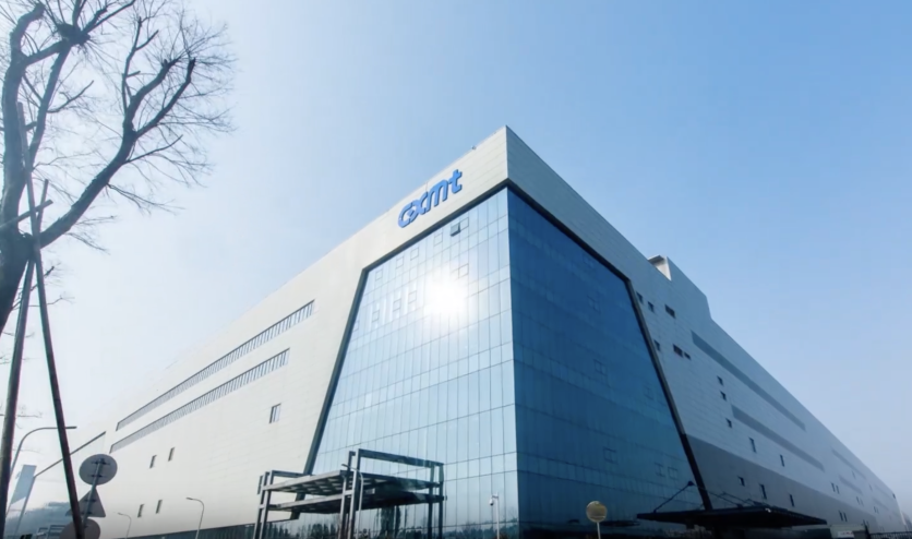
China's largest DRAM maker, ChangXin Memory Technologies (CXMT), is set to begin trading Monday on the Shanghai Stock Exchange's STAR Market — the close of a fundraising that pulled ¥57.9 billion (approximately $8.55 billion; exchange rate as of July 25, 2026; conversions are approximate) from investors and drained enough cash from China's secondary equity markets to knock the STAR 50 Index down nearly 20% from its July 1 peak. What CXMT does with that capital will determine whether it can close a technology gap that is measured not in ambition but in nanometers and wafer starts — and a compliance designation that already limits where those chips can go.
The offering — priced at ¥8.66 per share (approximately $1.28) — is Asia's largest IPO of 2026. It is also the largest semiconductor listing ever on the STAR Market, the Nasdaq-style board Beijing launched in 2019 specifically to channel public capital into technology companies it deems strategically important. If an overallotment option is fully exercised, total proceeds could reach ¥66.6 billion (approximately $9.84 billion).
For context on what the incumbents are spending: Samsung Electronics' fiscal 2026 total planned investment exceeds ¥110 trillion Korean won — approximately $73.3 billion at current rates — surpassing 100 trillion won for the first time. Micron Technology's fiscal 2026 capital expenditures are expected to exceed $25 billion, more than 80% above the prior year. SK Hynix completed a $26.5 billion Nasdaq share sale ten days before CXMT's subscription window opened. The combined incumbent spend is roughly fourteen times CXMT's haul before overallotment.
Why the STAR 50 Fell 20% Before CXMT Traded a Single Share
China's IPO mechanics require investors to freeze application funds until share allocations are settled and refunds processed. In the weeks before a major debut, investors often liquidate existing holdings to raise subscription capital — amplifying selling pressure on secondary markets. The STAR 50 Index fell nearly 20% from its July 1 high by the time the subscription window closed on July 16.
Peter Alexander, founder of advisory firm Z-Ben Advisors, described the dynamic without hedging: capital is unambiguously being pulled from the market in preparation for CXMT's public listing. He expects the dislocation to be temporary — projecting a sharp bounce on the first day of trading, possibly the second as well, before the broader market finds a new equilibrium.
Tim Sun, senior researcher at financial services firm HashKey Group, placed a specific number on investor expectations: the market anticipates CXMT's valuation will exceed ¥1 trillion (approximately $147.7 billion) after listing begins, a figure that would push it into a tier occupied by a small handful of global semiconductor companies.
Donnie Teng, Greater China semiconductor analyst at Nomura, argued the structural case for absorption: as long as AI infrastructure spending continues to drive hyperscaler capital expenditures, the memory supply it requires will sustain demand that can eventually absorb whatever short-term liquidity the IPO pulled from Chinese equities.
Others cautioned that the STAR 50 slide reflects deeper issues — crowded positioning and elevated leverage in A-shares — for which the CXMT listing is an amplifying factor rather than the root cause.
From ¥19 Billion Loss to ¥300 Million in Daily Profits — in Two Years
The commercial case for the stampede is straightforward. CXMT posted a net loss of ¥19.23 billion (approximately $2.84 billion) in 2023. By 2025, the company swung to its first annual profit. In Q1 2026, it reported revenue of ¥50.8 billion (approximately $7.51 billion) — a 719% year-on-year surge — and attributable net profit of ¥24.76 billion (approximately $3.66 billion). The company projects first-half 2026 net profit of between ¥50 billion and ¥57 billion (approximately $7.39 billion to $8.42 billion), which analysts have translated to roughly ¥300 million (approximately $44 million) in daily earnings.
That turnaround has a structural cause that is also a structural risk. When Samsung, SK Hynix, and Micron redirected advanced production capacity toward high-bandwidth memory for AI accelerators, they effectively vacated portions of the commodity DRAM market — DDR5 and LPDDR5X for PCs, smartphones, and servers — and CXMT stepped in to fill that gap. The resulting supply squeeze sent mainstream DRAM prices sharply higher. Gartner projected in February 2026 that combined DRAM and SSD prices would surge roughly 130% by year-end 2026. CXMT is the direct beneficiary of its larger rivals choosing margin over volume.
Its current global DRAM market share stands at approximately 8% as of Q1 2026, placing it fourth worldwide — behind Samsung at roughly 38%, SK Hynix at 29%, and Micron at approximately 22%. Its implied market capitalization at IPO pricing is approximately ¥579 billion to ¥588 billion (approximately $85.6 billion to $86.9 billion).
How CXMT Makes Chips Without the World's Most Advanced Equipment — and What That Costs
The single most consequential engineering fact about CXMT is that it has built its entire production roadmap without access to EUV lithography — the extreme ultraviolet machines that Samsung, SK Hynix, and Micron use to print the finest circuit features on leading-edge memory chips.
Here is the technical distinction that matters: ASML's EUV systems use 13.5-nanometer-wavelength light to expose chip circuitry in a single pass, achieving the finest feature sizes with high yield. ASML has never shipped an EUV machine to China, and Dutch export regulations — maintained under US pressure since 2019 — prohibit it from doing so.
CXMT compensates with an older technology called deep-ultraviolet multi-patterning. Its tools use 193nm-wavelength light and print circuits by running each layer through two to four separate exposure passes — a technique called self-aligned double patterning or self-aligned quadruple patterning (SADP/SAQP). Each additional pass accumulates tiny overlay errors and adds manufacturing steps, which reduces yield rates and raises cost-per-bit relative to single-pass EUV production.
CXMT's current leading process node — its internally labeled "G4" generation — achieves a cell size of roughly 16 nanometers, equivalent to the "1Z-class" used by the leading DRAM makers around 2018–2019. That places the process-node gap at approximately five to six years at current leading nodes. Seoul Economic Daily and independent analyst firm TechInsights both place the DDR gap at approximately two to three process generations for current shipping products.
The practical cost of that gap: CXMT's cost-per-bit still trails Samsung, SK Hynix, and Micron by more than 30%. In a normalized DRAM price environment — after the AI-driven supercycle ends and the incumbents' expanded capacity comes online — that cost disadvantage could compress CXMT's margins sharply.
Read more: CXMT IPO Draws 212× Oversubscription: What China's DRAM Bet Gets Right and Wrong
Bonded DRAM: CXMT's Unexpected EUV Workaround
The EUV constraint is not a simple binary ceiling, and the most significant unreported development around CXMT's IPO is that the company is actively testing a third pathway around it. Korean newspaper Hankgyung reported earlier in July that CXMT has begun pilot production of bonded DRAM at its Hefei facility — an architecture that separates the memory cell array and the peripheral control circuitry onto two distinct wafers, then fuses them together using wafer-to-wafer (W2W) hybrid bonding.
The engineering logic: each of the two wafers can be patterned individually using DUV multi-patterning at their respective achievable nodes. Because the array and logic sit on separate substrates, the combined device achieves density and performance gains that no single DUV-patterned wafer could reach on its own. The result is an architecture that approximates the functional advantage of EUV-enabled density without requiring EUV equipment.
Samsung is pursuing a similar architecture under its internal "B1b" project, and SK Hynix has its own parallel program. Korean media reports cited by Hankgyung suggest assessments that CXMT may currently hold an edge over its Korean rivals in both the bonded DRAM technology itself and the pace of development — a finding that, if accurate, would be one of the more surprising reversals in recent semiconductor history.
Bonded DRAM remains a pilot-stage technology at CXMT, with mass production years away. But its existence matters to anyone who treats "no EUV access" as a permanent hard ceiling on CXMT's trajectory: the correct framing is not a ceiling, but a constraint with multiple active engineering workarounds under development simultaneously.
The HBM Gap: Three Years Behind and Closing Faster Than Expected
High-bandwidth memory is the format the AI industry actually cares about, and it is where CXMT trails most clearly. HBM stacks multiple DRAM dies vertically using through-silicon vias — copper pillars drilled through the silicon of each die — and packages the resulting stack directly adjacent to an AI accelerator on a silicon interposer. The architecture delivers memory bandwidth of roughly 1 terabyte per second, versus approximately 50 gigabytes per second for conventional DDR5. That 20-fold difference is why Nvidia's AI accelerators demand HBM rather than DDR.
SK Hynix commands approximately 56–63% of the global HBM market. Samsung and Micron hold most of the rest. CXMT is at the sample-delivery stage for HBM3, with samples provided to Huawei for AI accelerator evaluation. Of CXMT's approximately 265,000 monthly wafer starts, fewer than 2% — roughly 5,000 wafers — are currently allocated to HBM production, with that share projected to reach 55,000 by end-2027. Samsung and SK Hynix are already racing toward HBM4 mass production — 16-layer stacking at the next performance tier.
Seoul Economic Daily, citing multiple industry sources, placed the overall HBM technology gap between South Korea's leaders and CXMT at approximately three years — narrowed from more than five years in earlier estimates — as Beijing's state-directed capital and technology acquisition have accelerated development. The TSV stacking process that HBM requires is less directly dependent on EUV patterning than flat lithographic scaling, which means CXMT's DUV constraint is more manageable in advanced packaging than it is in process-node advancement.
By end-2026, CXMT is projecting approximately 350,000 twelve-inch wafer starts per month — approaching Micron's roughly 375,000 — representing one of the fastest cleanroom-construction rates in the industry's history, with CXMT reportedly completing new cleanrooms in approximately 12 months versus the industry-standard 21–24 months.
What $8.55 Billion Buys — and What It Faces
CXMT has allocated the base ¥57.9 billion (approximately $8.55 billion) raise across three main areas: approximately ¥7.5 billion (approximately $1.11 billion) for manufacturing production-line technology upgrades; ¥13 billion (approximately $1.92 billion) for DRAM technology upgrades; and ¥9 billion (approximately $1.33 billion) for forward-looking research and development. The company is expanding production facilities in Shanghai and Beijing in addition to its primary Hefei campus.
Chairman and founder Zhu Yiming has committed to a ten-year post-listing lock-up period on his shares — an unusually long commitment that signals personal confidence in a sustained upswing — and has voluntarily allocated 768 million personally awarded shares for employee incentives.
Strategic investors confirmed in the offering include Alibaba Cloud Feitian, Meituan, and Xiaomi — a cross-section of China's technology consumer ecosystem that reflects the domestic downstream market CXMT is positioned to serve.
Apple, notably, is not among them. The Financial Times reported on July 8, 2026 that Apple had begun active qualification testing of CXMT's LPDDR5X chips for devices sold in China, while simultaneously leading a lobbying effort among US technology companies to seek White House and Commerce Department assurances that CXMT would not be designated on the Entity List. No supply agreement has been announced, and the lobbying effort is ongoing.
Read more: DDR5 RAM Hits $375 Floor for PC Builders: HBM Takes Three Times More Wafers
China's Intelligence Laws Apply Regardless of Where CXMT Ships
CXMT is a business-to-business chip supplier. Its DRAM modules do not independently collect or transmit end-user data — they store and process data at the direction of the host device. That distinction matters for consumer privacy, but it does not remove the legal framework that governs CXMT's obligations under Chinese law.
China's National Intelligence Law, enacted in 2017, requires all organizations and citizens under its jurisdiction to "support, assist, and cooperate with national intelligence efforts" under Article 7. Article 14 separately authorizes intelligence agencies to demand that cooperation. The Counter-Espionage Law (2014) adds that organizations and individuals must provide requested information truthfully and cannot refuse. China's Cybersecurity Law (2016) and Data Security Law (2021) impose additional data localization and government-access obligations — all of which apply to CXMT regardless of its newly listed public status.
These obligations apply regardless of CXMT's stated corporate governance, its newly listed public status, or the physical location of any servers. State-owned shareholders held approximately 36.29% of CXMT's equity before the IPO, and China's national semiconductor investment fund is a major investor.
For enterprise buyers evaluating CXMT memory for government contracts, defense-adjacent systems, or sensitive workloads: the compliance exposure arrives in two layers. The National Intelligence Law is the underlying structural condition — present regardless of any US action. The Section 1260H designation adds a US-government-specific layer: effective June 30, 2026, the Department of Defense is prohibited from procuring goods or services from CXMT-listed entities; effective December 23, 2027, all federal agencies are barred from procuring semiconductor products from CXMT, its subsidiaries, affiliates, and successors under Section 5949 of the FY2023 NDAA.
Enterprises that supply the US government — or aspire to — face a direct supply-chain conflict if they incorporate CXMT components into products destined for government procurement. CXMT also carries elevated risk of additional designation on Treasury and Commerce restricted lists; the MATCH Act, passed by the House Foreign Affairs Committee in April 2026, would extend the DUV export ban specifically to CXMT and ban ASML from servicing its existing installed equipment base.
Performance Gaps Incumbents Will Not Close for CXMT
The four dimensions that enterprise and institutional buyers should weigh alongside CXMT's genuine scale gains:
Process-node and cost economics: CXMT's cost-per-bit trails Samsung, SK Hynix, and Micron by more than 30%. That gap is sustainable at supercycle prices; it is not sustainable in a normalized DRAM market. The company's own prospectus acknowledges gaps in production capacity, research and development depth, and revenue scale relative to the incumbents.
HBM yield and volume: Fewer than 2% of CXMT's monthly wafer starts produce HBM. Samsung cleared NVIDIA qualification for its 16-layer HBM4 and began mass production first in 2026. SK Hynix and Micron hold the other 95%+ of global HBM supply. CXMT's HBM3E volume production target is 2027.
Ecosystem friction for international buyers: CXMT's DUV-produced chips are qualified by OEMs like HP, Dell, Acer, and Asus for devices sold outside the United States — a deliberate compliance firewall that demonstrates international qualification is achievable but that US-addressable market exposure remains limited. Documentation, support infrastructure, and tooling for enterprise integration lag the incumbents.
Independent benchmark verification: CXMT's DDR5-8200 modules have been validated on mainstream platforms. Consumer-level gaming performance is competitive with Samsung and SK Hynix equivalents at current specifications. However, CXMT has not publicly disclosed yield rates for its leading-node DDR5 production, and enterprise-grade qualification data from independent third parties at leading server workloads remains limited. Benchmark claims that appear in state-backed Chinese media should be treated as unverified until confirmed by named independent auditors.
The First-Day Print and What Comes After
Monday's listing ceremony is Beijing's most visible display yet of its semiconductor self-sufficiency strategy — a political event as much as a financial one. Government officials and senior figures from CXMT's upstream and downstream supply chain are expected on the exchange floor. The listing ceremony takes place on the Shanghai Stock Exchange floor Monday morning, Shanghai time (Sunday evening ET in the United States), as confirmed in the company's official listing announcement. A strong first-day open validates the state's narrative of a semiconductor sector coming of age; a quiet debut invites scrutiny of whether the AI-driven memory supercycle has already priced in perfection.
The question that will outlast the first-day price action: can CXMT convert its extraordinary revenue trajectory into sustained technological parity with its Korean and American rivals — without access to the world's most advanced chipmaking equipment, under a US national-security designation that limits where its products can go, and against incumbents spending more than a decade's worth of CXMT's current annual revenue on capital expenditures this fiscal year alone.
China's semiconductor memory market is projected to expand significantly in 2026 as AI infrastructure drives storage requirements, with computing and data-storage applications accounting for a large share of total regional demand growth. CXMT is the most visible embodiment of that bet — the only domestically owned DRAM manufacturer with the scale to realistically aspire to double-digit global market share. Its trajectory over the next five years, shaped by bonded DRAM development, HBM yield progress, and whether the MATCH Act's DUV restrictions become law, will be one of the defining technology contests of the decade.
For buyers, investors, and supply-chain planners: cost-per-bit is what CXMT offers. What it comes with is a process-node lag, a US national-security designation with expanding procurement consequences, and a legal obligation under Chinese intelligence law that no corporate governance structure removes. The first-day pop will get the headlines on Monday. The trajectory of those four variables will determine whether it matters five years from now.
Frequently Asked Questions
When does CXMT begin trading, and what happens to the STAR 50?
CXMT is scheduled to begin trading on the Shanghai Stock Exchange's STAR Market on Monday, July 27, 2026 — 9:30 AM Shanghai time, which corresponds to Sunday evening ET in the United States. The STAR 50 Index fell approximately 20% from its July 1 peak as investors liquidated existing holdings to fund IPO subscriptions, a standard mechanism in China's IPO system where applicants freeze cash until allocations are settled. Z-Ben Advisors' Peter Alexander expects a sharp first-day bounce for CXMT stock before both the shares and the broader market settle into a new equilibrium.
How does CXMT make competitive DRAM chips without EUV lithography?
CXMT uses deep-ultraviolet multi-patterning — specifically self-aligned double and quadruple patterning (SADP/SAQP) — to approximate the feature sizes that EUV-equipped rivals achieve in a single exposure pass. Each additional patterning pass adds manufacturing steps and overlay errors, which raises cost-per-bit relative to EUV production. CXMT's current leading node is roughly 16nm cell size, approximately two to three process generations behind Samsung and SK Hynix. Additionally, CXMT is piloting bonded DRAM — an architecture that separates the memory cell array and peripheral circuitry onto two wafers that are then fused together — which can achieve density gains without EUV by patterning each wafer individually at achievable DUV nodes.
What does CXMT's DoD military-company designation mean for buyers in 2026 and 2027?
The Pentagon's Section 1260H designation, formally restored on June 8, 2026, prohibits the US Department of Defense from contracting with CXMT-listed entities effective June 30, 2026. Products incorporating CXMT components may be ineligible for US government procurement contracts. Starting December 23, 2027, Section 5949 of the FY2023 NDAA extends the prohibition to all federal agencies, barring procurement of any semiconductor products from CXMT, its subsidiaries, affiliates, and successors. Buying CXMT DRAM is not prohibited for private-sector US companies, but any company that supplies the government — or plans to — faces a supply-chain conflict now.
What is CXMT's biggest technical obstacle beyond EUV access?
High-bandwidth memory yield. HBM requires stacking eight or more DRAM dies using through-silicon vias — copper pillars drilled vertically through each die — and is the format Nvidia AI accelerators demand. CXMT has achieved HBM3 technology parity on paper, according to Seoul Economic Daily, but fewer than 2% of its monthly wafer starts currently produce HBM. Samsung and SK Hynix are already in mass production of HBM4. CXMT's target for HBM3E volume production is 2027, placing it approximately three years behind the leaders in the segment that generates the highest margins and the most AI infrastructure revenue.

-
 C114 Communication Network
 -
 Communication Home
