
 Search

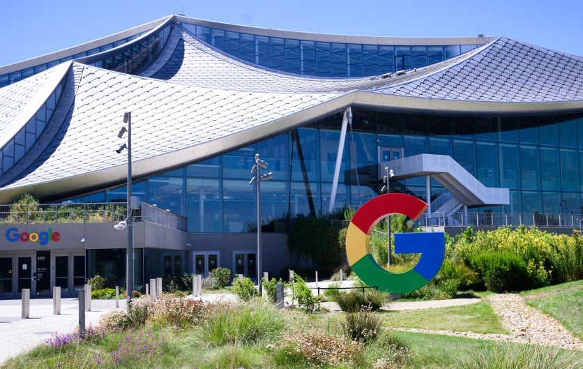
A giant Google logo is seen at Google's Bay View campus in Mountain View, California on August 13, 2024 where the "Made by Google" media event was held today. JOSH EDELSON/AFP via Getty Images
The day NVIDIA announced a $3.5 billion investment in Taiwan's MediaTek, binding the Taiwanese chip designer into its NVLink Fusion ecosystem, another investor quietly joined the same bond offering: Alphabet. The disclosure would have been easy to miss — MediaTek's statement named Alphabet and "other investors" without dollar amounts, as confirmed by CNBC's September 2026 coverage — but it turns out to be the most analytically significant detail in a deal that generated enormous coverage focused almost entirely on the wrong question.
The conventional framing of the NVIDIA-MediaTek deal asks: will AI infrastructure standardize on NVLink Fusion, the proprietary interconnect that NVIDIA controls, or UALink, the open standard backed by AMD, Intel, Google, Microsoft, Meta, and approximately 85 other companies? That framing assumes the two paths are mutually exclusive and that hyperscalers are choosing sides. Alphabet's co-investment in the MediaTek bond offering is the single most precise piece of evidence available that this framing is wrong.
Alphabet is a UALink Consortium founding member alongside AMD, Broadcom, Cisco, HPE, Intel, Meta, and Microsoft. It helped write the UALink specification. It is simultaneously paying MediaTek to design the TPU v8i (codename Zebrafish) — Google's cost-optimized AI inference chip — through a design partnership announced at Google Cloud Next 2026. And then, on August 31, 2026, it also co-invested alongside NVIDIA in the $3.9 billion MediaTek convertible bond offering that formalized MediaTek as NVLink Fusion's primary XPU integration gateway for hyperscalers. Alphabet is simultaneously on all three sides of a supposedly binary competition. That is not confusion; it is a deliberate portfolio strategy, and it is the signal that TechTimes readers building or procuring AI infrastructure need to understand before making any interconnect commitment.
What NVIDIA Bought With $3.5 Billion
The mechanics of NVIDIA's investment matter because they reveal what the company is actually optimizing for. NVIDIA purchased convertible bonds — not equity — representing approximately 90% of MediaTek's record $3.9 billion offering, the largest of its kind in Taiwan's capital market history. A convertible bond pays a fixed return (or in some structures, zero coupon) in exchange for the bondholder's right to convert into equity at a predetermined price. NVIDIA's financial return on the bond appreciates most if MediaTek's stock rises — which happens if MediaTek's AI chip business grows — which happens if hyperscalers use MediaTek to design custom accelerators that connect into NVLink Fusion. The financial instrument and the technology strategy are the same bet.
What NVIDIA received in exchange is MediaTek's commitment to offer NVLink Fusion as the design foundation for custom AI accelerators — called XPUs — that MediaTek builds on behalf of hyperscalers and other large customers. A hyperscaler that brings a custom compute die to MediaTek for production now receives a chip pre-equipped with NVIDIA's UCIe bridge chiplet, which connects the custom silicon to NVIDIA's NVLink fabric without requiring the hyperscaler's engineering team to independently master NVIDIA's proprietary interconnect specification.
The deal also deepens the companies' prior collaborations. MediaTek co-designed the GB10 Grace Blackwell Superchip at the heart of NVIDIA's DGX Spark personal AI supercomputer, contributing the CPU cores and memory controller while NVIDIA provided the GPU die and the NVLink chip-to-chip interconnect. Future generations of both DGX Spark and RTX Spark — NVIDIA's Arm-based computing platform for Windows laptops targeting consumers and developers — will continue to be developed jointly through a roadmap detailed in NVIDIA's official announcement. Jensen Huang, NVIDIA's founder and CEO, called MediaTek "one of the world's great semiconductor companies." MediaTek's vice chairman and CEO Rick Tsai called the investment a strengthening of a relationship "spanning cloud AI infrastructure, local AI computing, and automotive in the era of physical AI."
How NVLink Fusion Actually Works — and What NVIDIA Keeps
Understanding what hyperscalers get — and what they give up — when they adopt NVLink Fusion requires looking at the three layers of the platform.
At the die-to-die level, custom accelerators and XPUs connect to NVIDIA's fabric through a UCIe bridge chiplet. UCIe (Universal Chiplet Interconnect Express) is an open industry standard for die-to-die communication within a chip package. NVIDIA's NVLink Fusion chiplet receives UCIe signals from the custom die on one side and translates them to NVLink protocol on the other side — meaning chip designers work in the open UCIe standard and NVIDIA's proprietary protocol is encapsulated within the chiplet. The custom compute die never needs to implement NVLink itself.
At the chip-to-chip level, NVLink-C2C provides bidirectional bandwidth of 300 GB (gigabytes) per second for connections between CPUs and GPUs or CPUs and XPUs. This is the same interconnect used in the GB10 SoC.
At the rack level, NVIDIA's sixth-generation NVLink switch fabric connects up to 72 XPUs in a single all-to-all domain at 3.6 TB (terabytes) per second per XPU, with an aggregate bandwidth of 260 TB per second across the full domain and end-to-end latency three times lower than Ethernet as documented in NVIDIA's developer blog.
What NVIDIA does not share: the NVLink Switch chips themselves, the PHY layers, and the communication controllers that regulate the fabric. Every XPU in the NVLink Fusion ecosystem must connect to an NVIDIA product to access the network. The platform is open to custom compute dies; it is not open to custom switching. That architectural choice is NVIDIA's economic requirement for participating in the custom silicon economy at all — it ensures that even when a hyperscaler substitutes NVIDIA GPUs with its own custom chips, NVIDIA still collects revenue from the switch trays, ConnectX NICs, BlueField DPUs, or Vera CPUs in the same rack.
Moor Insights analyst Matt Kimball, vice president and principal analyst at Moor Insights and Strategy, named the choices plainly: scale-up Ethernet, NVLink Fusion, and UALink. For hyperscalers evaluating which path to take, those three options remain, but the production reality narrows the choice considerably.
What NVHBM Adds to the Dependency Stack
NVIDIA also announced a new memory architecture alongside the AWS Trainium4 partnership on August 26 — one week before the MediaTek deal — that extends its proprietary influence from the interconnect layer into the memory subsystem. NVHBM (NVIDIA High-Bandwidth Memory) moves the HBM memory controller off the XPU's compute die and embeds it directly into the HBM base die, the foundational layer of the three-dimensional memory stack.
In every AI accelerator built on today's JEDEC HBM4e standard, the logic that manages communication between the processor and its memory stacks sits on the processor die and consumes silicon area that could otherwise hold compute units. NVHBM eliminates that constraint by relocating the controller into the memory package itself. According to NVIDIA's NVHBM architectural specifications, the result is a 67% reduction in PHY and interface area on the XPU compute die, up to 25% more of the compute die available for differentiated compute logic, 30% greater memory bandwidth versus standard HBM4e, and 15% lower HBM power consumption, for a stated 30% improvement in end-to-end XPU performance.
At data center scale, the power savings compound. A data center operating at one gigawatt with 2,000-watt accelerators could theoretically accommodate approximately 15,000 additional XPUs within the same power envelope from NVHBM's memory efficiency alone — compute capacity added not by adding power but by spending memory power more efficiently.
Amazon's Annapurna Labs, which designs the AWS Trainium custom AI training chip series, is the first announced customer collaborating on NVHBM for Trainium4. Under that arrangement, Trainium4 silicon would connect into the same NVLink fabric as NVIDIA GPUs, enabling rack-scale systems where AWS-designed accelerators and NVIDIA chips operate alongside each other, connected by a common high-bandwidth fabric. AWS is simultaneously a UALink founding board member. It is running both paths, just as Alphabet is.
One caveat that procurement teams should note: as of September 2026, every NVHBM performance specification is an architectural figure from NVIDIA, not a measurement from a shipping product. as of September 2026, no independent NVHBM benchmarks exist. AWS's early collaboration provides an external signal that at least one major customer has evaluated and found the architecture credible, but NVHBM remains pre-production. Treat its figures as architectural targets until independently verified on silicon.
Alphabet Sits on the UALink Board and Just Co-Invested in NVIDIA's NVLink Fusion Partner
Alphabet is a founding board member of the UALink Consortium, which it helped form in May 2024 alongside AMD, Broadcom, Cisco, HPE, Intel, Meta, and Microsoft. The UALink Consortium, founded in May 2024, was designed as an open alternative to NVIDIA's proprietary NVLink — a vendor-neutral specification that multiple hardware companies can implement, so that hyperscalers are not structurally dependent on NVIDIA's switch silicon to scale their accelerator pods.
UALink 2.0, published in April 2026, adding In-Network Compute provisions to the original specification, now has more than 85 member companies. The technical capability is real: UALink supports up to 1,024 accelerators within a single pod at 200 Gbps per lane. The open-standard architecture means that if AMD, Intel, Astera Labs, and other hardware vendors produce conforming switch silicon, any hyperscaler can run a scale-up AI fabric without touching an NVIDIA product.
The current commercial reality is that purpose-built UALink switch silicon from Astera Labs and other partners was not at production scale as of September 2026. AMD's Helios rack platform — which uses UALink as its interconnect standard — ships its H2 2026 systems using UALink-over-Ethernet (UALoE), a bridge solution that runs the UALink protocol over an 800 GbE (gigabit Ethernet) physical layer, because native UALink silicon is not yet production-ready. TechTimes' AMD Helios coverage documents the open-standard interconnect approach and Azure's commitment to deploy it. The openness is structurally and contractually real; the specific hardware implementation in 2026 relies on Ethernet PHY components as an interim bridge.
This is the production timeline that makes NVIDIA's NVLink Fusion strategy viable: the window during which NVLink Fusion is the only production-ready, pre-validated option for hyperscalers that want to connect custom XPUs to a proven rack-scale AI fabric. Every XPU program that commits to NVLink Fusion during this window adopts an interconnect dependency that would require a full platform teardown to remove, and by the time UALink commercial silicon ships broadly, those programs will already be generating production inference traffic.
Alphabet's co-investment in the MediaTek bond is legible against this backdrop. Co-investing in the dominant production-ready option while maintaining governance stakes in the open standard's specification body is not a contradiction — it is the rational hedging behavior of an organization that knows it cannot predict which interconnect standard will dominate at scale two chip generations from now. The same is true for AWS, which is simultaneously a UALink board member and a Trainium4/NVLink Fusion partner. The hyperscaler strategy is to preserve optionality at every layer, even when that means funding what appear to be competing standards.
What makes Alphabet's case particularly sharp is the third data point: MediaTek is also designing Google's TPU v8i (Zebrafish), the cost-optimized inference chip announced at the Google Cloud Next TPU v8i announcement in April 2026. That chip uses a different interconnect architecture from NVLink Fusion, and will be manufactured at TSMC on its 2nm process with production targeting 2027. Counterpoint Research's MediaTek 2028 forecast projects MediaTek will capture 26% of AI ASIC server compute shipments by 2028, approaching 5 million units, driven substantially by TPU v8i Zebrafish and its successor programs. That volume projection has almost nothing to do with NVLink Fusion — it is primarily a function of Google's own TPU deployment scale.
In other words: MediaTek will become one of the largest AI chip designers in the world primarily by designing Google's TPU chips, and secondarily by acting as NVIDIA's XPU integration gateway for other hyperscalers' NVLink Fusion programs. Both things are true simultaneously. Alphabet is a co-investor in the entity doing both.
MediaTek's Market Position Before and After the NVIDIA Deal
MediaTek's AI chip division reported revenue of $2 billion for 2026 with the total addressable market for custom AI silicon at $80 billion by 2027. The broader custom silicon market is growing faster than merchant GPUs: according to TrendForce's ASIC growth forecast for 2026, custom ASIC chip sales are projected to increase 44.6% in 2026 compared with 16.1% growth for GPU shipments. ASIC-based AI server shipments are expected to reach approximately 27.8% of the market in 2026 — the highest share since 2023.
Against that backdrop, MediaTek is competing to displace Broadcom as the dominant ASIC design services provider — or at least to establish itself as a credible second option. Broadcom's current position is formidable: it designs the training-optimized TPU v8t (Sunfish) for Google and maintains design partnerships with Meta, Microsoft, and OpenAI programs. Google alone is estimated to spend approximately $8 billion per year with Broadcom on TPU development.
MediaTek's NVLink Fusion gateway role opens a different market segment from the Broadcom TPU relationship. Broadcom's dominance is in pure custom ASIC design services — designing the compute die itself for hyperscalers with large enough programs to justify the investment. MediaTek's NVLink Fusion role is in XPU integration services — providing the surrounding infrastructure (memory interfaces, interconnect chiplets, packaging, rack validation) to hyperscalers and chip design teams that want to focus their engineering on a differentiated compute die without independently qualifying NVIDIA's entire interconnect stack. These are different customers at different stages of custom silicon maturity, and they are not mutually exclusive of each other or of MediaTek's Google TPU design work.
The NVIDIA investment deepens MediaTek's access to capital and aligns NVIDIA's financial interests with MediaTek's success in this market. At NVIDIA's current revenue scale — $59.7 billion in net income in Q2 FY2027 alone — a $3.5 billion convertible bond is a strategic instrument, not a stretch. The comparable recent deployments: a $2 billion stake in Marvell, as confirmed in the NVIDIA Marvell partnership announcement, which also adopted NVLink Fusion; NVIDIA's $5 billion Intel investment as part of a custom data center CPU collaboration announced September 2025; and the 2019 announcement of the Mellanox acquisition for approximately $7 billion, which gave NVIDIA the InfiniBand networking infrastructure from which NVLink's data center ambitions later grew. Each investment followed the same logic: deepening technical integration with a strategic partner through financial alignment.
What Custom Silicon Builders Should Take From All of This
For enterprise teams and infrastructure architects evaluating AI accelerator strategies, the Alphabet data point reframes the decision they face. The question is not "should we adopt NVLink Fusion or UALink?" It is "what is our exposure to each, and how do we manage it?"
Hyperscalers at the scale of Google, AWS, and Microsoft can answer that question by funding both paths simultaneously — co-investing in the dominant production-ready interconnect while maintaining governance positions in the open alternative. That portfolio approach is not available to most organizations. Smaller cloud providers, AI labs, and enterprises without the engineering resources of a hyperscaler face a more constrained choice: a NVLink Fusion XPU program delivers production-ready rack integration today, at the cost of structural dependency on NVIDIA switch silicon for as long as that program runs; a UALink program delivers architectural independence from NVIDIA, at the cost of waiting for commercial switch silicon that is not yet at production scale.
The two dimensions that matter most for this decision are time and replaceability. If a team needs custom silicon in production racks in 2026 or early 2027, NVLink Fusion is the validated path. If a team is willing to operate with a bridge solution (UALink-over-Ethernet) in the near term and wait for native UALink switch silicon, the architectural independence is real — but the timeline requires patience that hyperscalers with production inference revenue pressure often cannot afford. Meanwhile, NVIDIA's window to lock in the NVLink Fusion standard before UALink commercial hardware ships is precisely what the MediaTek investment is designed to extend: more hyperscaler XPU programs starting on NVLink Fusion means more installed infrastructure that cannot be easily migrated to a different interconnect standard, even after UALink switch silicon becomes widely available.
The NVHBM layer adds a third dimension. A hyperscaler XPU program that adopts NVHBM alongside NVLink Fusion now has NVIDIA's proprietary architecture present at both the interconnect layer and the memory layer. That is a deeper integration than the interconnect dependency alone, and it provides NVIDIA with economic participation in the custom silicon program whether or not NVIDIA's GPU sits in the same rack at all.
The point is not that NVLink Fusion is a trap — its technical credentials are strong, its production-readiness advantage is real, and its performance figures, while pre-production for NVHBM, are grounded in established semiconductor engineering. The point is that Alphabet, the hyperscaler that best understands what it means to run a multi-generational AI chip program, chose not to rely on any single one of the available options. It is paying to keep all of them open.
Frequently Asked Questions
Why would Alphabet invest in a MediaTek NVLink Fusion bond offering if Alphabet helped found the UALink Consortium to compete with NVLink?
The apparent contradiction resolves when you recognize that hyperscalers at Alphabet's scale are not picking an interconnect standard — they are engineering optionality across all available paths. UALink provides long-term architectural independence from NVIDIA: any hardware vendor can build conforming switch silicon, and no single company controls the protocol. But UALink commercial switch hardware was not at production scale as of September 2026, and hyperscalers cannot pause AI infrastructure deployment to wait for a specification body to produce commercial hardware. NVLink Fusion is production-ready now. Alphabet co-investing in MediaTek's bond offering is consistent with a strategy of maintaining UALink governance to shape the open standard's long-term direction while also ensuring access to the production-ready system today. The two bets are not contradictions; they are portfolio positions across different time horizons.
What does "every NVLink Fusion system must include an NVIDIA product" actually mean for a hyperscaler building its own custom AI chip?
It means the hyperscaler can design whatever compute die it wants — the chip's matrix multiply engines, vector units, cache hierarchy, and specialized processing blocks are entirely up to the design team — but the chip will operate in a rack that includes NVIDIA's NVLink Switch trays, NVIDIA's ConnectX NICs, or NVIDIA's Vera CPU, all of which NVIDIA sells and prices. The custom compute die is the hyperscaler's; the surrounding infrastructure fabric is NVIDIA's. This is the economic arrangement NVIDIA describes as "interoperability" — and it is what critics describe as a toll-booth structure. NVIDIA participates in the economics of every accelerator deployment regardless of whether an NVIDIA GPU is the primary compute engine.
How does MediaTek's role in Google's TPU v8i (Zebrafish) design relate to its new NVLink Fusion partnership with NVIDIA?
These are two distinct relationships that happen to involve the same partner company. MediaTek is designing Google's TPU v8i Zebrafish inference chip under a separate design partnership announced at Google Cloud Next 2026. That chip does not use NVLink Fusion, and will be manufactured at TSMC on its 2nm process with production targeting 2027. MediaTek's NVLink Fusion partnership with NVIDIA, formalized August 31, serves a different customer set: hyperscalers and AI labs that want to bring their custom XPU designs to MediaTek and receive chips pre-validated for NVIDIA's rack-scale AI factory. The two roles are not in conflict — MediaTek is building a position as a general-purpose ASIC design services provider for hyperscalers of all interconnect persuasions, which is structurally different from Broadcom's relationship with any single hyperscaler.
Will UALink eventually displace NVLink Fusion, or will both interconnect standards coexist long-term?
The most likely outcome, given Alphabet's and AWS's portfolio behavior, is coexistence — at least through the next two to three chip generations. UALink provides structural incentives for hyperscalers that need to negotiate NVIDIA's pricing from a position of credible alternatives; NVLink Fusion provides production-readiness advantages that hyperscalers under time pressure to deploy cannot ignore. The interconnect industry has historical precedent for this: Ethernet and InfiniBand coexisted in data centers for more than a decade before Ethernet's cost advantages drove widespread adoption for most workloads while InfiniBand retained its position in high-performance computing. Whether UALink follows a similar trajectory depends on when commercial switch silicon reaches production scale and whether its real-world performance in heterogeneous racks matches its specification advantages on paper.

-
 C114 Communication Network
 -
 Communication Home
