
 Search

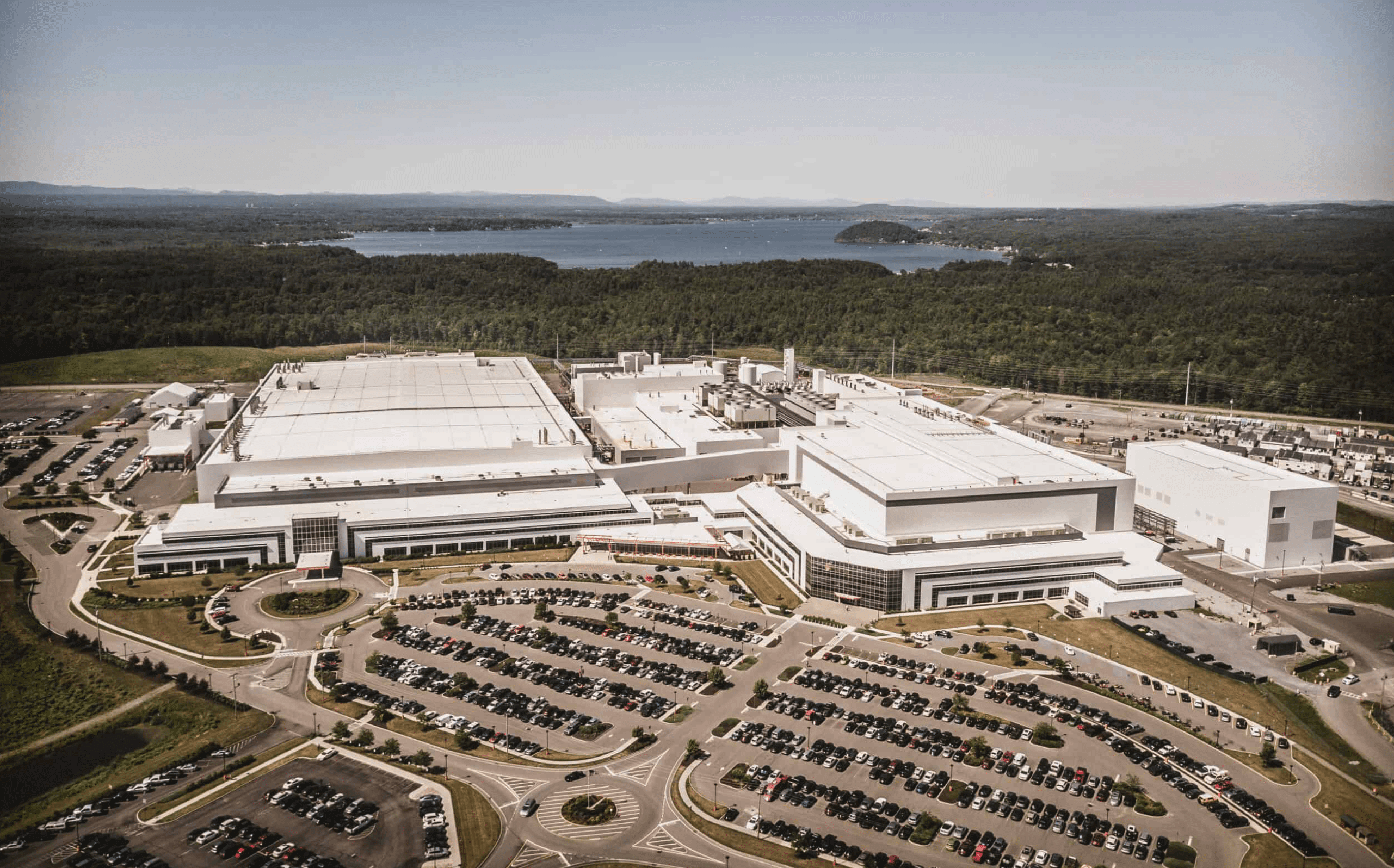
GlobalFoundries will supply the technology and operate two planned semiconductor fabs in Malta, New York, under a U.S.–Japan initiative providing up to $21 billion in funding. Japan will finance construction, while the United States and Japan will jointly own the facilities. An initial investment of approximately $10 billion will support the first fab, with a second investment of roughly $10 billion contemplated for another facility. The Semiconductor Industry Association identifies the project as the first semiconductor investment under the bilateral Strategic Investment Initiative.
The first 300mm fab is expected to begin operating in 2029. Separately, GF and the U.S. Department of Commerce agreed to reallocate $955 million from the company’s existing CHIPS and Science Act award toward silicon photonics, silicon-germanium (SiGe) and advanced packaging investments in Malta and Burlington, Vermont. Commerce will also receive approximately 4% equity in GF under a separate agreement.
The structure gives GF an operating and technology-licensing role alongside government-backed ownership of the new manufacturing assets. Reuters reports that GF will earn construction, operating and licensing fees, manage customer relationships, and initially serve customers including Renesas Electronics and Apple. GF remains majority-owned by Mubadala Investment Company.
| GLOBALFOUNDRIES · U.S.–JAPAN INITIATIVE | |
| Up to $21 Billion | |
| Two planned fabs. Expanded U.S. chip capacity. | |
| LOCATION | Malta, New York |
| FUNDING MODEL | Japan funds construction U.S.–Japan joint ownership; GF supplies technology and operates the fabs. |
| PHASED INVESTMENT | Approximately $10B for the first fab. A further approximately $10B would fund the second. |
| CAPACITY PER FAB | ≈900,000 300mm wafers annually at full operation. |
| FIRST FAB TIMELINE | 2026 · Groundbreaking expected 2029 · Operations targeted |
| NETWORKING & AI INFRASTRUCTURE | |
| $955M CHIPS Reallocation | |
| Existing award funding redirected toward technology investments in Malta, New York, and Burlington, Vermont. | |
| Silicon Photonics SiGe Advanced Packaging | |
| Source: GlobalFoundries and Semiconductor Industry Association, October 14, 2026. Investment, capacity and operating dates reflect announced plans; the second fab depends on additional investment. | |
“GF was selected because fabs of this scale require more than capital,” said Tim Breen, CEO of GlobalFoundries.
Analysis
GlobalFoundries’ New York initiative sits within a broader expansion of manufacturing capacity, process technologies and advanced packaging across its global network. In June 2025, GF outlined a $16 billion investment plan for New York and Vermont, combining more than $13 billion in previously planned expansion and modernization with an additional $3 billion for research and development, including photonics, packaging and GaN. The new Japan-funded fab structure changes how additional capacity will be financed and operated. The earlier and latest investment figures should not simply be added together without clarification of their overlap.
GF is also expanding its European manufacturing base. Its €1.1 billion SPRINT project in Dresden targets annual capacity exceeding one million 300mm wafers by the end of 2028. Alongside that expansion, GF plans to develop and manufacture FDX Fusion, an FD-SOI platform targeting 7nm-like digital performance with analog, RF and embedded-memory capabilities for Physical AI. Development remains subject to German government approval under the proposed support framework. In Singapore, GF’s manufacturing partnership with Monolithic Power Systems targets additional power-management chip production beginning in early 2027. These programs extend GF’s capacity across connectivity, power, sensing and embedded computing.
Japan is simultaneously financing semiconductor capacity overseas and rebuilding advanced manufacturing at home. Rapidus’ IIM-1 facility in Chitose, Hokkaido, began pilot-line operations in April 2025 and targets mass production of 2nm gate-all-around logic in 2027. Rapidus reported verification of transistor operation on 300mm wafers and delivery of a pre-release process design kit to early customers. Its parallel Rapidus Chiplet Solutions program is developing advanced packaging, including 2.xD and 3D integration. The remaining work includes improving yield and validating the production systems required to move from pilot manufacturing into commercial output.
TSMC provides another major expansion path through its majority-owned Japan Advanced Semiconductor Manufacturing subsidiary in Kumamoto. The first fab entered volume production at the end of 2024. TSMC subsequently upgraded its plans for the second facility to include 3nm technology for AI-related demand; in its April 2026 earnings call, management scheduled volume production for 2028. That represents a substantial evolution from the original second-fab announcement, which targeted operation by the end of 2027.
Taken together, these projects illustrate Japan’s participation across several layers of semiconductor manufacturing: Rapidus is developing a domestic advanced-logic foundry, TSMC is bringing established foundry processes into Japan, and the GF initiative finances additional U.S. capacity supported by an existing operator. For AI infrastructure, the strategic significance extends across processors, optical connectivity, power-management devices and packaging. Announced investment establishes the manufacturing opportunity; process qualification, customer adoption, yield and production ramps determine when that capacity becomes usable supply.
| Company Profile: GlobalFoundries | |
| Business | Contract semiconductor manufacturing across differentiated process technologies. |
| Headquarters | Malta, New York, United States |
| Leadership | Tim Breen, CEO; Thomas Caulfield, Executive Chairman |
| Founded | 2009 |
| Ownership | Nasdaq: GFS; majority-owned by Mubadala Investment Company. |
| Technologies | Silicon photonics • SiGe • FD-SOI • RF • FinFET • advanced packaging |
| Manufacturing | Operations across the United States, Europe and Asia. |
| Coverage | Semiconductors • optical interconnects • AI infrastructure • data centers • automotive • industrial electronics |

-
 C114 Communication Network
 -
 Communication Home
