
 Search

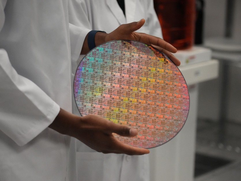
An employee holds a silicon wafer with chips etched into it at Applied Materials in Sunnyvale, California, on May 22, 2023. JIM WILSON/POOL/AFP via Getty Images
America is building the most expensive and consequential industrial infrastructure in a generation — and is on track to not have enough people to run it. A landmark joint analysis by McKinsey & Company, the SEMI Foundation, and the National Science Foundation projects that the US semiconductor industry faces a shortfall of up to 157,000 workers by 2030. The shortage does not reflect a generational shortage of engineers. About 52 percent of engineering graduates take engineering roles each year — but of those, only 3 percent choose semiconductor manufacturing. That means approximately 1,500 engineers enter the chip industry annually, against a projected demand of 88,000 semiconductor engineers by 2029.
The math is simple and brutal: AI and software companies are competing for the same graduate cohort and winning by a ratio of roughly 33 to 1. No amount of fab construction changes that ratio on its own.
"I'm concerned," Jon Taylor, Executive Vice President of Samsung's semiconductor division in Austin, Texas, told CNBC this week. "We just don't see that there's enough technical people in the pipeline."
Why Fabs Cannot Train Their Way Out of a Competition Problem
The semiconductor workforce gap has two distinct and compounding components, and conflating them leads to the wrong interventions.
The first is a pipeline problem: the US semiconductor manufacturing workforce declined 43 percent from peak employment levels in 2000, and the industry lost decades of hands-on cleanroom expertise as manufacturing offshored to Taiwan, South Korea, and China. Community college programs, university partnerships, and federal workforce funds are rebuilding that pipeline — but slowly. More than 80 community colleges have launched or expanded semiconductor programs since the CHIPS and Science Act passed in 2022, aided by a $200 million federal workforce development fund from SEMI. McKinsey's updated 2026 analysis estimates that projected supply will reach approximately 62,000 workers against a total demand of 189,000 — leaving the 127,000-to-157,000 gap.
The second component is the competition problem, and it is harder to solve. A university graduate choosing between a process-engineering role at a fab in the Arizona desert and a software position at a San Francisco AI lab is not just comparing salaries — they are comparing working conditions, commute flexibility, cultural prestige, and the perceived trajectory of each industry. US chip fabs typically pay $127,000 to $187,000, with senior engineers earning more. These are strong salaries by any measure. But top AI-lab compensation packages often exceed them substantially, add remote-work flexibility, and carry social status that semiconductor manufacturing — with its mandatory on-site cleanroom shifts — simply cannot match for most graduates.
This is why McKinsey's analysis found that 53 percent of semiconductor workers considered leaving their jobs in 2023, up from 40 percent in 2021. The shortage is not just an incoming pipeline problem — it is also an outgoing retention problem in a sector where one-third of the existing workforce is 55 or older.
The practical consequence: even programs that successfully add engineers to the pipeline must run fast merely to keep pace with attrition, and the net supply against demand barely moves.
What Cleanroom Skills Actually Require — and Why Online Training Cannot Substitute
Understanding why the workforce gap is so stubborn requires understanding what cleanroom semiconductor manufacturing actually demands.
A modern fabrication plant is built around interdependent precision processes: photolithography, which uses extreme ultraviolet light to etch circuit patterns at sub-7-nanometer scale; chemical-mechanical planarization (CMP), which polishes wafer surfaces to atomic-level flatness between process layers; thin-film deposition; and ion implantation. Each process runs in an environment where a single particle of airborne contamination can destroy an entire wafer batch. The machines involved — EUV lithography steppers from ASML cost upward of $200 million each — are not available in university labs.
This creates a training bottleneck that no online curriculum resolves. McKinsey's research identifies the irreducible minimum: engineers and technicians require hands-on proficiency with production-grade equipment before they are useful inside a fab. Purdue University's Birck Nanotechnology Center — which celebrated its 20th anniversary in 2025 — is among a small number of US university facilities with real cleanroom infrastructure capable of providing that preparation. The standard graduate pipeline, without access to such facilities, produces engineers who understand semiconductor theory but cannot operate a fab tool without months of supervised on-site training.
This explains why the construction timeline for a US fab — 24 months from groundbreaking to initial production — is roughly twice what it takes in Taiwan (12 to 16 months). The gap is not primarily a permitting difference. It reflects the absence of a dense local ecosystem of workers who have operated similar equipment, and the resulting longer ramp time before a new hire can contribute independently.
The Buildout That Depends on Workers Who Do Not Yet Exist
The scale of the American semiconductor buildout is genuinely unprecedented.
TSMC broke ground on its first Arizona fab in 2021, and that facility has been in volume production of its N4 process since late 2024, with yields matching Taiwan fabs. TSMC's second Arizona fab, using 3-nanometer process technology, has completed construction, with volume production expected in 2027. In July 2026, TSMC announced an additional $100 billion investment to build at least four more fabs dedicated to 2-nanometer and below processes, bringing its total Arizona commitment to $265 billion across 10 fabs and two advanced packaging facilities.
TSMC has responded to the talent shortage by building its own pipeline: the company visited about a dozen universities in 2025 and is working to convert hundreds of interns into full-time hires to help fill approximately 6,000 open roles at its Arizona campus. The effort is real — and still well short of the need.
Intel's Ohio One plant, initially announced as America's largest fab complex, is now expected to begin production between 2030 and 2031. Samsung's first Taylor, Texas, fab — the first of two facilities in a roughly $37 billion Texas expansion — is targeting risk production by late 2026, with approximately 3,500 jobs once fully operational. Because domestic engineering expertise is still limited, Samsung and SK Hynix have been temporarily importing South Korean engineers to jumpstart operations at their new US fabs.
Memory is expanding as well. Micron is building a fab in Boise, Idaho, beginning wafer production in 2027, and has broken ground on a $100 billion campus in the Syracuse, New York area. SK Hynix has begun construction of its first American high-bandwidth memory packaging plant in West Lafayette, Indiana, directly serving the AI data center supply chain.
Taylor Roundtree, a McKinsey partner who led the workforce analysis, put the situation plainly: "There's just not enough talent to go around. Folks are realizing that the potential gap is so large that they collectively have to solve it."
What the Education Response Has Produced — and What It Has Not
The response from universities and the federal government has been real, and genuinely larger than most past workforce development efforts.
Purdue University launched its Semiconductor Degrees Program in 2022, offering a campus-wide semiconductor certificate accessible to all undergraduates, departmental concentrations across multiple engineering departments, and online master's programs. The program runs through Purdue's Birck Nanotechnology Center and its affiliated SCALE program, a $45 million Department of Defense initiative that expanded to 22 universities and 48 industry and government partners. Purdue interim president Mitch Daniels, who has championed semiconductor education at Purdue since hosting US Secretaries of State and Commerce at the Birck Center in 2022, told CNBC this week: "If we don't move more quickly and aggressively than we have before, we will lose."
In May 2026, the SEMI Foundation launched the NNME's first four regional nodes, activating a national network of more than 325 organizations — K-12 school districts, community colleges, universities, workforce development agencies, and semiconductor employers — across four regional hubs led by the Arizona Commerce Authority, Boise State University, NY Creates, and the University of Texas at Austin. Each node is eligible for up to $20 million in NSF funding over five years. The NNME announced the formation of its inaugural Industry Advisory Committee in mid-September 2026, drawing senior leaders from semiconductor manufacturers, universities, and community colleges to guide its national workforce strategy.
Industry has added direct investment. Samsung has donated millions of dollars to the University of Texas, Texas A&M, and the University of Illinois for chip engineering programs, put $1 million toward technical labs at Taylor High School near its fab, and hosts more than 100 interns annually. Intel launched an apprenticeship program in Arizona in 2024 and pledged $50 million in scholarships across more than 80 Ohio institutions near its fab under construction there. Purdue also built and operates the Chipshub platform, providing free online chip design simulation tools via nanoHUB, developed with Cadence, Synopsys, Siemens, the Department of Defense, and the National Science Foundation.
McKinsey's modeling is candid about the result: these programs, even if they fully hit their stated targets, will avert a long-term technician shortage but will not close the engineer gap. Engineer training programs take four or more years to produce a graduate who can contribute independently in a fab — and annual demand growth for semiconductor engineers is forecast to peak at 20,000 per year in 2027, far faster than any educational pipeline can ramp.
Is the Policy Environment Stable Enough to Sustain the Buildout?
One dimension the original McKinsey/SEMI report does not fully address is the shifting federal policy environment.
In August 2025, the Trump administration converted $5.7 billion in unpaid CHIPS Act grants owed to Intel — combined with $3.2 billion from the Defense Department's Secure Enclave program — into an $8.9 billion federal equity stake representing a 9.9 percent ownership position in Intel. The administration simultaneously voided $7.4 billion in Natcast funding, removing Natcast as operator of the National Semiconductor Technology Center and transferring control to the National Institute of Standards and Technology. These restructurings suggest the CHIPS Act framework is not static, and the workforce development funding streams tied to it are subject to the same uncertainty.
Additionally, H-1B visa tightening under the current administration has reduced the stopgap that US semiconductor manufacturers historically used to supplement domestic talent shortfalls with foreign-born engineers, many of them trained at US universities. The NNME's regional node architecture is explicitly designed to develop domestic talent rather than rely on immigration-based relief — a strategic choice that reflects the new policy environment and imposes a longer timeline to results.
Can Fabs Become More Culturally Competitive for Graduates?
McKinsey's research and the industry's own response suggest that the selection-rate problem requires more than training infrastructure — it requires changing how semiconductor careers are perceived by the students who are choosing AI and software instead.
The industry has tried direct outreach. Internship programs at TSMC, Samsung, and Intel are designed partly to expose students to fab work before they make permanent career choices. Purdue's Chipshub platform puts chip design simulation in the hands of any university student with a browser. Samsung's Taylor High School lab partnership aims to introduce semiconductor concepts at the secondary level, before students' career identity solidifies around AI and software.
Whether these efforts can shift a 33-to-1 selection ratio is genuinely unknown. The oil-and-gas industry provides a cautionary parallel: despite high salaries and abundant jobs, it faces historic attrition because students associate it with an industry in long-term decline. The semiconductor industry's trajectory is clearly the opposite — demand is accelerating, not declining — but the cultural perception gap is real and documented. McKinsey's Organizational Health Index data shows that half of US semiconductor companies score below the median benchmark on talent development, working environment, and capture of external ideas. That is a retention and attraction problem that compensation alone does not solve.
The fabs are being built. The machines will arrive. The question — the only one that actually constrains the timeline — is whether the engineers will follow.
Frequently Asked Questions
How many semiconductor engineers does the US actually produce each year, and why is it so few?
About 1,500 engineers enter semiconductor manufacturing annually in the US. This is not because the US produces too few engineers overall — roughly 52 percent of engineering graduates take engineering roles each year — but because only 3 percent of engineering graduates choose semiconductor manufacturing. The remainder opt for AI, software, data science, and adjacent fields, which offer remote work, higher social prestige at many universities, and compensation packages that can exceed fab salaries for top graduates. The 3 percent figure is a selection rate, not a supply problem. Changing it requires changing the perceived relative attractiveness of chip manufacturing careers — not just producing more engineering graduates.
Why is the 157,000-worker gap projected to peak in 2030, and what happens if it is not closed by then?
The 2030 figure reflects the point at which the CHIPS Act–funded fab buildout reaches its full planned production capacity. Fabs under construction across Arizona, Texas, Ohio, New York, and Indiana are all expected to reach full production ramp between 2026 and 2030. If the worker gap is not substantially closed by then, the consequences are production delays, underutilized facility capacity, extended reliance on temporary imported talent, and — at the macro level — a strategic failure of the CHIPS Act's core rationale: making the US less dependent on foreign semiconductor supply. Fabs that cannot hire enough process engineers cannot reach full production yield, regardless of the capital invested in their construction.
What can engineers and students do right now if they want to work in semiconductor manufacturing?
The fastest entry paths are through university programs with direct industry partnerships and guaranteed-interview tracks. TSMC runs a Technician Apprenticeship Program and a 10-day Semiconductor Technician Quick Start program through Maricopa Community Colleges in Arizona that accepts applicants without prior fab experience. Purdue's Semiconductor Degrees Program offers undergraduate certificates and online master's programs through its Birck Nanotechnology Center, which has one of the largest university cleanrooms in the US. GlobalFoundries runs paid, roughly 18-month apprenticeships in Malta, New York, in collaboration with Hudson Valley Community College. Purdue's Chipshub platform also provides free online chip design simulation access for any student. Pay for entry-level fab technicians typically starts above $50,000 and rises steeply with experience; process engineers with undergraduate degrees start above $90,000, with senior engineers earning substantially more.
Will importing temporary workers from South Korea and Taiwan solve the short-term gap?
It is a stopgap, not a solution. Samsung and SK Hynix are currently importing South Korean engineers temporarily to jumpstart operations at their new US fabs. This addresses the immediate need to commission and calibrate equipment, but it is expensive, logistically complex, and does not build the domestic talent base that the CHIPS Act's national security rationale requires. H-1B visa tightening under current immigration policy further limits how long or broadly this strategy can scale. The NNME regional node architecture is specifically designed to reduce dependence on imported talent by building a domestic pipeline rooted in the communities where fabs are located — Arizona, Ohio, New York, Indiana, Texas. Whether that pipeline produces results before the 2030 deadline remains the central unanswered question.

-
 C114 Communication Network
 -
 Communication Home
