

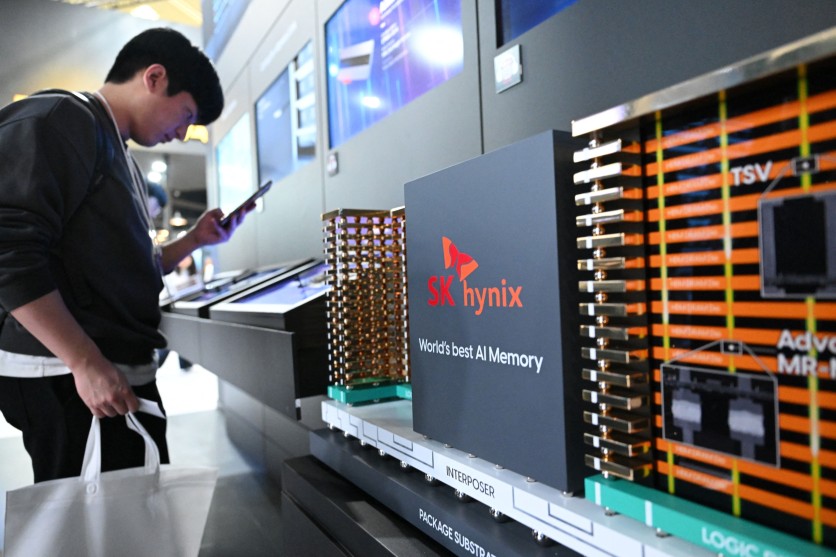
A visitor takes a picture of a model of SK hynix's high-bandwidth memory (HBM) technology during the 2025 World IT Show in Seoul on April 24, 2025. South Korean chip giant SK hynix reported record quarterly profits on April 24, thanks to soaring global demand for artificial intelligence, highlighting the firm's ability to weather mounting tariff threats. JUNG YEON-JE/AFP via Getty Images
SK hynix has shipped samples of its seventh-generation high-bandwidth memory, HBM4E, in a 12-layer configuration — moving earlier than planned and setting up a tightening race with Samsung Electronics, which sent its own samples weeks ago.
The company said on June 18 that, drawing on its mass-production experience across HBM3, HBM3E, and HBM4, it delivered the 12-stack HBM4E samples to major customers and would work closely with them to reach mass production on schedule and ease bottlenecks in AI systems. The shipment came earlier than the second-half timeline SK hynix had given on its first-quarter earnings call in April; it had previewed the product at Computex 2026 in early June.
What HBM4E Actually Improves
HBM is the stacked DRAM that sits beside an AI accelerator and feeds it data fast enough to keep the processor busy — the tightest bottleneck in the AI compute chain — so each generation's gains translate fairly directly into how hard a chip can be pushed. HBM4E improves on HBM4 through changes to the DRAM core die, interface design, and manufacturing process.
By SK hynix's account, it applied its 10nm-class sixth-generation "1c" DRAM for the first time, where HBM4 used the prior 1b, on a 32-gigabit (4GB) core die that lifts capacity density about 50% over HBM4. Stacked 12 high, that yields 48GB per stack, up from 36GB for 12-layer HBM4. The number of I/O pins is unchanged at 2,048, but per-pin speed reaches up to 16 gigabits per second — as much as 45% faster than the roughly 11–13Gbps before — delivering about 4 terabytes per second of bandwidth per stack, which industry estimates put 38–50% above HBM4. Energy efficiency improved more than 20%.
The Base Die Is Where the Two Rivals Diverge
SK hynix did not disclose the base-die specification, but the industry understands it to be built on TSMC's 3nm-class process — a step up from the 12nm-class base die used through the previous generation. That detail is unconfirmed by the company, but it points to the most telling difference between the two Korean rivals.
The base die is the HBM's control layer, the logic chip at the bottom of the stack that handles reads, writes, and error correction for each DRAM layer and governs the package's overall speed and stability. Moving it to a more advanced node lets that controller run faster and cooler, which is why the choice of who makes it is strategically loaded. SK hynix is understood to buy its base die from TSMC; Samsung makes its own on its 4nm-class foundry process — a make-versus-buy split that reflects two different bets on how to win the generation.
To hold the 12 layers together, SK hynix uses its Advanced MR-MUF packaging — bonding the dies with a heat-dissipating epoxy molding compound via reflow and then a thermal-compression bonder — and says process optimization cut thermal resistance about 17% versus HBM4, helping a dense stack run without throttling.
Read more: Samsung Pursues Nvidia HBM4E Supply and LP40 Foundry Work After Seoul Bilateral
Why Sampling First Matters — and Why It Doesn't Settle Anything
The timing matters because HBM4E is expected to power next year's flagship AI chips, including Nvidia's Rubin Ultra and AMD's Instinct MI500. Rubin Ultra is slated to carry 384GB of HBM per GPU — eight of the 48GB 12-layer parts — up more than 30% from the 288GB on the HBM4-based Vera Rubin. Sampling first gives a supplier a head start in the customer qualification and optimization that decide volume orders.
But a head start is not a win, and in this market the distinction is sharp. SK hynix led the HBM market with a 58% share in the first quarter, according to Counterpoint Research, with Samsung and Micron at about 21% each, and its shares jumped to a record intraday high after the announcement. Even so, the demand picture is unusually narrow: SK Group's own chairman noted at Computex that only one customer — Nvidia — is currently asking for HBM4E, and analysts have stressed that in a market shaped by a single dominant buyer, who ships samples first matters far less than whom Nvidia ultimately chooses to buy from. Samsung shipped its first 12-layer HBM4E samples on May 29, weeks before SK hynix, and the order race is still to be run.
The Two Korean Rivals, Head to Head
Ahn Hyun, SK hynix's president and chief development officer, said applying the company's accumulated technology and mass-production capability to HBM4E lays the groundwork to keep leading AI innovation, and that SK hynix would strengthen its position as a "full-stack AI memory" maker — a reference to its full portfolio of memory for AI systems.
Samsung, for its part, used the same 32Gb 1c DRAM but with a base die on its own 4nm-class foundry process, and says it has secured yield and mass-producibility and will pursue supply on customers' schedules. With both having now sampled, the contest moves to the part that actually decides the generation: whose parts clear customer qualification cleanly and whose capacity ramps on time.
Read more: Samsung Ships Industry-First HBM4E Samples: 3.6 TB/s Bandwidth Beats SK Hynix by Six Months
Frequently Asked Questions
What is HBM4E?
HBM4E is the seventh generation of high-bandwidth memory, a type of DRAM that stacks multiple memory dies vertically and sits next to an AI accelerator to feed it data at very high speed. SK hynix's 12-layer HBM4E reaches 48GB per stack and up to 16 gigabits per second per pin, delivering about 4 terabytes per second of bandwidth, with more than 20% better energy efficiency than the previous HBM4.
What is the difference between HBM4 and HBM4E?
HBM4E is an enhanced version of HBM4. SK hynix's HBM4E uses a denser sixth-generation "1c" DRAM core die (versus HBM4's "1b"), raising per-stack capacity from 36GB to 48GB, lifts per-pin speed to as much as 16Gbps from the roughly 11–13Gbps range, and improves energy efficiency by more than 20%, while keeping the same 2,048 input/output pins.
What is the base die in an HBM stack?
The base die is the logic chip at the bottom of an HBM stack that controls the memory above it — managing reads, writes, and error correction and setting much of the package's speed and stability. Building it on a more advanced process node lets it run faster and cooler. SK hynix is understood to use a TSMC 3nm-class base die, which it has not officially confirmed, while Samsung makes its base die on its own 4nm-class foundry process.
Who leads the HBM market?
According to Counterpoint Research, SK hynix led the high-bandwidth memory market with a 58% share in the first quarter of 2026, with Samsung and Micron each at about 21%. SK hynix has also been the primary HBM supplier to Nvidia. Samsung is competing aggressively for the next generation and shipped its first 12-layer HBM4E samples ahead of SK hynix, but the volume orders for HBM4E have not yet been decided.
-
 C114 Communication Network
 -
 Communication Home
