Search


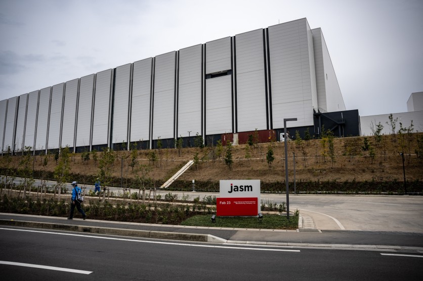
PHILIP FONG/gettyimages.com
Japan's Ministry of Economy, Trade and Industry formally approved a revised production plan for TSMC's second fabrication plant in Kumamoto Prefecture on October 16, 2026, certifying what will become Japan's first facility capable of manufacturing 3-nanometer logic semiconductors. The approval is a genuine milestone — but the story behind the numbers is more technically revealing than the headline suggests. The original plan called for 48,000 wafers per month at 6nm and 12nm. The approved plan calls for 6,000 wafers per month at 3nm. That 87.5% capacity reduction is not a setback. It is a direct consequence of what 3nm manufacturing actually requires — and of who makes the equipment that enables it.
Japan's Node Upgrade — and the Volume Reckoning It Reveals
When TSMC first laid out plans for the Kumamoto second fab in February 2024, the blueprint called for producing 6nm and 12nm chips at a monthly capacity of 48,000 wafers, according to the JASM second fab announced in 2024 — a volume-first approach geared largely toward Japan's automotive and industrial sectors. Under the now-approved plan, the facility will produce 3nm chips at an initial monthly target of just 6,000 wafers, an 87.5% reduction in output volume compared to the prior design. METI approved the plan change on October 16.
The reduction is not a sign of diminished ambition. It reflects what happens when a facility moves from mature-node mass production into frontier-node manufacturing. At 3nm, a chip requires extreme ultraviolet (EUV) lithography — a technology that prints circuits with light at a wavelength of just 13.5 nanometers (0.000000053 inches), roughly one-fifteenth of a wavelength of visible light. EUV lithography is used on more than 20 critical layers at the 3nm node, compared to approximately 14 layers at 5nm. And only one company in the world is the sole manufacturer of EUV systems at commercial scale: ASML, the Dutch equipment maker.
TSMC and METI framed the revised plan explicitly around the requirements of 3nm manufacturing, which demands EUV equipment and carries a significantly heavier investment burden per wafer than the more mature nodes it replaces. METI's Director of the Information Industry Division, Tomonari Nanbu told reporters that "given the progress of AI transformation, 3nm cutting-edge logic semiconductors that power AI are indispensable," signaling that the ministry views the node upgrade as a strategic necessity.
TSMC has indicated that the 6,000-wafer figure represents only the first phase, and that production capacity will expand depending on the level of additional government support it receives.
Why EUV Scarcity — Not Strategy — Governs the Capacity Figure
Understanding why the Kumamoto II fab will start at 6,000 wafers per month instead of 48,000 requires understanding EUV tool availability.
ASML's EUV systems — the NXE series, which uses an optical system with a numerical aperture of 0.33 — are the workhorses of every advanced-node fab in the world. Each machine uses EUV plasma generation technology in which a pulsed laser fires at liquid tin droplets more than 50,000 times per second, producing photons at the 13.5nm wavelength that then pass through a reflective optical system to print circuit patterns onto silicon wafers.
ASML produces roughly 50 to 60 EUV systems per year globally. Every major foundry — TSMC in Taiwan and Arizona, Samsung in South Korea, Intel in the United States, and now Rapidus in Hokkaido — competes for allocation from that limited production line. Each EUV tool costs in excess of $150 million; installing and qualifying a single tool at a new fab takes months. A 3nm production line requires multiple such tools running in concert.
The 6,000-wafer-per-month figure represents what EUV tool allocation and yield ramp-up can realistically support at a new Japanese site in the 2026–2028 installation window, given that TSMC is simultaneously prioritizing equipment for its Fab 21 Phase 2 in Arizona (targeting 3nm production in the second half of 2027) and its continued 3nm and 2nm expansion in Taiwan. There was earlier reporting of a 15,000-wafer monthly figure when Taiwan approved the 3nm investment in March 2026; the official METI-certified plan lists 6,000 wafers per month. METI's official documents do not explain the difference, but the discrepancy is consistent with a first-phase ceiling set by tool availability rather than demand.
METI is explicitly considering increasing its support, and METI included the subsidy request in its fiscal year 2027 preliminary budget — a process that will determine whether TSMC can raise the 6,000-wafer ceiling before mass production begins in December 2028.
Subsidy Structure and Investment Scale
METI designated the Kumamoto II plant as a subsidy recipient under Japan's semiconductor reindustrialization program. The government originally planned to provide ¥732 billion (approximately $4.6 billion) in subsidies tied to the prior 6nm/12nm plan. With the revised blueprint now approved, that figure has been adjusted to ¥645.15 billion (approximately $4.1 billion), reflecting the reduced initial production volume, as documented in the METI official revised plan document.
The first Kumamoto fab's subsidy was also revised downward — from ¥476 billion to ¥409.5 billion (approximately $2.6 billion). Between the two plants, total committed public support fell from ¥1.208 trillion to ¥1.055 trillion (approximately $6.7 billion). However, METI is considering increasing the second fab's support as the full scale of the 3nm investment becomes clearer. TSMC's own statement confirmed total Kumamoto capital spending exceeds $23 billion (approximately ¥3.63 trillion) across both facilities.
Timeline: December 2028
Commercial production at the second Kumamoto fab is targeted for December 2028. Under METI's certification conditions, JASM commits to ten-year operation and to increasing production in the event of a domestic shortage — conditions attached to all Japanese government semiconductor subsidies.
The 2028 production date means Kumamoto's 3nm node will come online approximately one year after TSMC's 3nm capacity at its second Arizona fab, where Arizona 3nm production targets 2027 in the second half. That sequence reflects TSMC's global capital allocation priorities — Taiwan first, then Arizona under US CHIPS Act pressure, then Japan — rather than any deficiency in the Japanese site itself.
Kumamoto I Also Revised
METI's October 16 approval package extended to the existing Kumamoto I plant as well. Originally planned to run both 12–16nm and 22–28nm processes at a combined 55,000 wafers per month, the first fab plan revised to 22-28nm phases out all 12–16nm production, concentrating the facility on 22–28nm nodes (plus 40nm processes reserved for Japanese domestic customers) at 45,000 wafers per month across the subsidized facility footprint, and 50,000 wafers per month across the full plant.
JASM attributes this revision to how automotive and industrial customer demand has evolved — an implicit acknowledgment that sluggish electric vehicle adoption has moderated demand for the advanced-mature nodes originally planned for Kumamoto I. The move effectively repositions Kumamoto I as a stable-node workhorse for Sony image sensors, automotive chips, and industrial electronics, freeing the second facility to serve as the campus's leading-edge AI-oriented anchor.
The first fab has been operating since late 2024, when volume production began at 12–28nm. Its resilience was tested on July 28, 2026, when a magnitude 7.1 earthquake halted JASM Fab 1 operations for equipment inspections. The facility recorded a maximum seismic intensity of 5 at the fab site; analysts estimated a one-week shutdown could represent approximately $14 million in potential lost revenue, according to the TSMC Kumamoto earthquake impact estimate. The fab subsequently returned to normal operations.
What 3nm Means: Density, Power, and Why Artificial Intelligence Drives It
A 3nm chip is not merely a faster version of a 6nm chip. The performance gap is structural. TSMC's N3 process delivers 70% logic density over 5nm, plus a 15% performance improvement at the same transistor count, and a 30% reduction in power consumption compared to its 5nm node — the previous generation widely used in high-performance AI chips.
For AI workloads — the inference and training pipelines that power large language models, image generators, and autonomous systems — transistor density and power efficiency are the primary engineering constraints. More transistors per square millimeter means more compute per die; lower power per transistor means larger dies can be built without exceeding thermal limits. The combination makes 3nm the node at which AI accelerators cross from constrained to capable at the scale AI infrastructure requires.
TSMC CEO C.C. Wei met Prime Minister Takaichi in Tokyo in February 2026 to signal the shift in direction, citing "strong demand driven by AI" as the driving rationale for moving the second Kumamoto fab from 6nm to 3nm. Japan's PM Office stated that "there is a huge significance to have the world's most advanced semiconductor factory in Japan from the perspective of economic security."
By installing 3nm capacity in Japan, TSMC can serve GPU and AI accelerator customers who require geographically diversified supply chains, while also positioning the facility to capture Japanese hyperscaler and defense-adjacent demand. JASM's ownership structure — TSMC holds 86.5% of JASM with Sony Semiconductor Solutions at 6%, Denso at 5.5%, and Toyota at approximately 2% — ensures that Japan's largest technology, automotive, and electronics companies have direct investment stakes in the outcome.
Japan's Two-Track Advanced Semiconductor Strategy
The approval places Japan in a position it has not held since the 1980s: a participant in frontier logic production. Outside of Taiwan and South Korea, no country currently hosts commercial 3nm production facilities. The Kumamoto II certification changes that calculus, making Japan a participant — if initially a modest-scale one — in the frontier of logic chip production.
Japan is simultaneously backing Rapidus Corp., the government-sponsored domestic foundry aiming to begin 2nm mass production in Hokkaido in the second half of 2027. METI has maintained that the two ventures are complementary rather than competitive, with Rapidus targeting a different customer base (smaller volumes, faster cycle times, and domestic design houses) versus TSMC Kumamoto's higher-volume production for global foundry customers.
In practice, both projects reflect Japan's determination to rebuild a semiconductor manufacturing base that atrophied significantly over the past two decades. The 1990s collapse of Japan's vertically integrated chip industry left the country almost entirely dependent on TSMC and South Korean suppliers for advanced logic — a dependence that the earthquake on July 28 briefly made visceral for the local supply chain. Kumamoto Governor Kimura's welcome of METI's approval reflected that regional context: the two-fab campus has already catalyzed significant investment in local infrastructure, housing, and supporting industries across Kyushu.
What Comes Next
The immediate path forward involves TSMC finalizing equipment installation plans for the second fab, with EUV tool procurement and facility fit-out expected to dominate 2027. METI's fiscal 2027 budget process will determine whether subsidy levels expand beyond the current ¥645.15 billion ($4.1 billion) baseline, which could in turn influence whether TSMC elects to raise the 6,000-wafer monthly ceiling before mass production begins.
For the global AI chip supply chain, the December 2028 production date is consequential: it represents a new node of 3nm capacity outside Taiwan at a moment when demand for advanced AI silicon is expected to remain in excess of available supply well into the next decade. At 6,000 wafers per month, Kumamoto II will not meaningfully close that gap. But as TSMC and METI have both made clear, the first phase is not the final chapter — it is the volume that EUV tool availability makes possible today, with future phases contingent on ASML production, subsidy finalization, and how quickly TSMC can qualify the new Japanese site to the same yield standards it achieves in Taiwan. That qualification process, not the political approval, is where the real engineering work lies.
Exchange rate as of October 2026; conversions are approximate.
Frequently Asked Questions
When will TSMC start producing 3nm chips in Japan?
Under the plan certified by Japan's Ministry of Economy, Trade and Industry, JASM's second fab in Kumamoto is scheduled to make its first 3nm shipments in December 2028. Commercial production officially begins that same month, with JASM committed under subsidy conditions to operating for a minimum of ten years.
Why is the initial production volume so much lower than the original plan?
The original 2024 plan called for 48,000 wafers per month at 6nm and 12nm — mature nodes achievable with deep ultraviolet (DUV) lithography equipment. The revised 3nm plan is certified at 6,000 wafers per month, because 3nm production requires extreme ultraviolet (EUV) lithography. EUV tools are produced by only one company (ASML, based in the Netherlands), at a rate of roughly 50–60 systems per year globally. Installing, qualifying, and ramping multiple EUV machines at a new site takes years. The 6,000-wafer figure reflects what EUV tool allocation can realistically support in the 2026–2028 window — not simply a strategic choice to start small.
How does Kumamoto II compare to TSMC's other 3nm facilities?
TSMC's primary 3nm production base remains in Taiwan (Fabs 18A, 18B, and 18C in Tainan). TSMC's Fab 21 Phase 2 in Arizona is expected to begin 3nm production in the second half of 2027 — approximately one year ahead of Kumamoto. Kumamoto's 6,000 wafers per month at launch compares to Arizona's production capacity of approximately 10,000–20,000 wafers per month at ramp. All are far smaller than TSMC's Taiwan capacity, which handles the majority of global 3nm logic demand for Nvidia, Apple, and AMD.
What does the Japanese government's subsidy commitment actually require TSMC to do?
Under METI's certification conditions, JASM commits to operating the second fab for a minimum of ten years and to increasing production in the event of a domestic semiconductor shortage. The subsidy is capped at ¥645.15 billion (approximately $4.1 billion) for the second fab — down from the ¥732 billion (approximately $4.6 billion) originally planned for the 6nm/12nm design. METI has included a request for potential additional subsidy funds in its fiscal year 2027 preliminary budget process, the outcome of which will determine whether TSMC can scale beyond the initial 6,000-wafer ceiling.

-
 C114 Communication Network
-
 Communication Home