Search


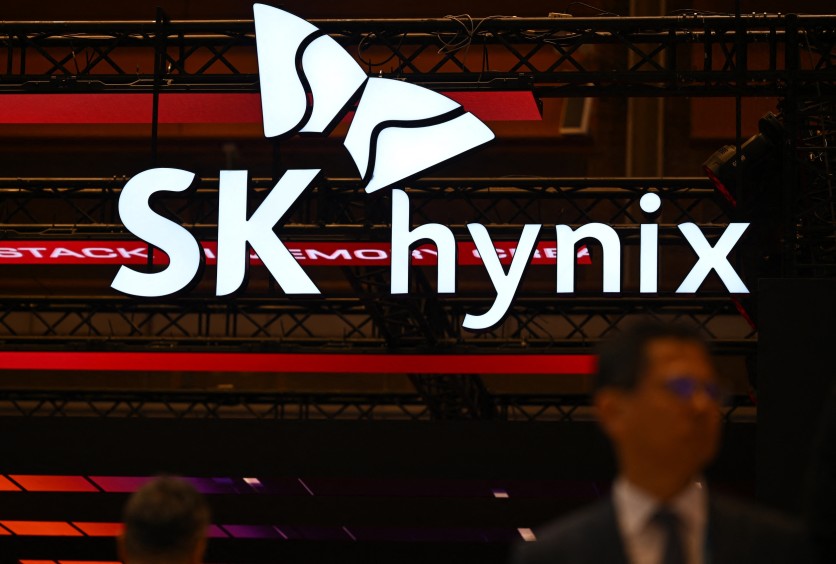
Jung Yeon-je / AFP via Getty Images
SK Hynix has formally unveiled a commercial product built on XCENA's MX1 chip, and Samsung co-authored the agentic AI memory architecture blueprint with the startup at OCP Global Summit 2026 — the clearest signal yet that CXL computational memory has crossed from conference demonstration to commercial ingredient. The SK Hynix CXL Hybrid Memory product, built directly on MX1, debuted at the SK Hynix summit booth while XCENA ran two live inference demonstrations across the show floor.
At the summit, held October 12–15 at the San Jose McEnery Convention Center, South Korean fabless startup XCENA demonstrated its MX1 chip — the industry's first CXL 3.2 computational memory device — while SK Hynix debuted its CXL Hybrid Memory at its own booth. By the time the show floor closed, XCENA had two of three largest DRAM makers publicly aligned behind its controller, mass production on Samsung foundry lines scheduled for the end of 2026, and revenue expected from 2027.
Two Demos, One Argument About Where the Real Bottleneck Lives
XCENA ran two live demonstrations at OCP, each aimed at a distinct pain point in large-scale AI inference.
The first showed multiple inference servers drawing from a single, shared key-value (KV) cache held in a CXL memory pool. A KV cache stores the context a language model has already processed so responses can be generated without recomputing prior tokens. In conventional deployments, every server maintains its own copy — a redundant pattern that multiplies DRAM requirements and floods interconnects with repeated data transfers. By pooling the KV cache through CXL, XCENA's approach keeps one authoritative copy that any server on the fabric can access via standard load/store operations, reducing both the memory footprint and cross-server traffic.
The second demonstration targeted retrieval-augmented generation (RAG), the dominant pattern for deploying large language models in enterprise settings. RAG pipelines run vector search — matching a user query against a potentially massive embedding index — before every inference call. Ordinarily that means shuttling large datasets from memory to the host CPU on every lookup. MX1 instead runs the vector search directly inside the memory device, using what XCENA calls its near-data processing (NDP) engine: thousands of custom RISC-V cores with FP32 and FP16 vector units embedded in the controller itself.
The chip's Hot Chips 2026 presentation quantified what that means in practice. Compared with a host CPU processing data over a standard CXL link, a single MX1 delivered up to 4.7× higher throughput and 18.7× greater energy efficiency across data-processing kernels representative of analytics and AI pipelines. Against a CPU reading from its own local DDR5 — the conventional performance baseline — MX1 still achieved up to 2× higher throughput and 6.2× greater energy efficiency.
What Does the MX1 Actually Do — and Why Does the Architecture Matter?
MX1 is a CXL 3.2 Type 3 device. That classification matters: a Type 3 CXL device exposes its attached memory to the host CPU as byte-addressable memory, accessible with standard load/store instructions — the same way the CPU accesses its own DRAM — without requiring any change to the application's programming model. The host simply sees a larger pool of memory on the CXL bus.
The chip connects via a PCIe 6.0 dual x8 interface. The dual-x8 design is not merely a bandwidth specification — it is a topology decision. In a dual-socket server, each x8 link connects to a different CPU socket, giving both processors a single-hop path to the MX1 memory. A single x16 link would force the second socket to route through the first socket's CPU interconnect, adding latency and contention at scale. Hyperscaler rack designs are predominantly dual-socket, making this a practical architectural consideration rather than a theoretical one.
MX1 supports up to 2 TB of DDR5 across four memory channels, using 256 GB DIMMs at two per channel. The NDP engine consists of 3,072 RISC-V cores organized in clusters of 32; each cluster shares an L2 cache and a data translation lookaside buffer (TLB). XCENA provides a standard C/C++/Rust toolchain via LLVM, so software teams do not need to write assembly or custom microcode to target the NDP cores.
The chip draws 40W at chip level, with the full board — four DDR5 DIMMs installed — reaching 90W. For a device that can replace multiple DRAM-laden servers in a pooled memory configuration, that power envelope is a critical datapoint for data center operators calculating total cost of ownership.
MX1 also includes a dedicated PCIe 6.0 root complex for attaching NVMe SSDs directly to the controller. XCENA markets this capability as InfiniteMemory: the SSD tier is exposed to the host CPU as byte-addressable CXL memory, with 64 KB page granularity and a 1,024-entry on-chip map cache that DRAM fronts as a warm tier. The effect is a memory hierarchy extending total addressable capacity far beyond what DRAM alone can economically provide — relevant for KV cache workloads where context windows are growing faster than DRAM price points are falling.
SK Hynix: From Joint Research to a Named Product
The most commercially concrete development from OCP was SK Hynix's formal unveiling of its CXL Hybrid Memory product, built directly on the MX1 chip. SK Hynix — the world's second-largest DRAM manufacturer — displayed the product at its own summit booth, a step beyond the reference-platform demonstrations the two companies had previously run together.
The CXL Hybrid Memory pairs MX1-managed DDR5 with InfiniteMemory's SSD-backed tier, delivering memory capacity scalability significantly beyond what conventional CXL DRAM modules can reach while outperforming raw SSD access. SK Hynix and XCENA are now jointly validating the architecture in real-world AI serving environments, with RDMA-based shared memory as the primary interconnect path under optimization — a lower-level integration than a typical hardware partnership, suggesting genuine co-engineering rather than a logo arrangement.
The collaboration makes commercial sense on structural grounds: SK Hynix brings DRAM and NAND manufacturing scale at the level a hyperscaler supply chain requires; XCENA brings the controller intelligence that transforms passive memory expansion into active computation. CXL memory expansion without a capable controller is limited by the host CPU's ability to orchestrate it — the same bottleneck MX1's NDP engine is designed to remove.
Samsung: Co-Authoring the Agentic AI Memory Blueprint
XCENA's relationship with Samsung operates on a different axis — less product-focused for now, more architectural — but anchored in two concrete facts: XCENA's founders are Samsung Electronics and SK Hynix veterans, and MX1 chips are scheduled for production on Samsung foundry lines by the end of 2026.
At OCP on October 15, XCENA Chief Product Officer Harry Kim co-presented with Samsung Electronics engineers in a session titled "Disaggregated CXL Memory Architecture for Agentic AI: Dynamic Pooling, Sharing, and PNM Offloading." The session addressed how disaggregating memory from compute — made physically practical by CXL's cache-coherent interconnect — can serve the particular demands of agentic AI systems, which require large, long-context memory pools that grow and shrink dynamically as agents spawn, pause, and terminate.
Samsung's OCP agenda was dense with CXL content independent of XCENA: sessions covered KV cache offloading to SSD, the evolution of its CXL Process-Near-Memory line, and Kubernetes-based orchestration for multi-node agentic AI. The co-session with XCENA was the most architecturally concrete overlap — alignment on pooling, sharing, and NDP offload as the three pillars of next-generation inference memory.
At Hot Chips 2026 in August, Samsung researchers described a pilot disaggregated memory system built in collaboration with XCENA and memory fabric company Liqid — a reference design combining GPU servers with MX1-equipped CXL memory nodes connected through a CXL switch. That working demonstration predates the OCP summit and indicates the partnership has been producing silicon-level results for several months.
What Separates MX1 From Competing CXL Controllers?
MX1 is not the only CXL memory controller announced in the past year, and the competitive distinction matters for understanding why SK Hynix and Samsung chose it as a platform anchor.
Astera Labs' Leo family and Marvell's Structera X 3406/3506 — the latter announced October 12, the same week as OCP — are CXL smart-memory controllers focused on memory expansion, pooling, and sharing. They use Arm-based processor cores optimized for orchestration and management. MX1's 3,072 RISC-V cores — organized in 96 clusters of 32 — represent a fundamentally different architectural bet: not a smart controller that manages passive memory, but a memory device capable of running substantial data-processing workloads autonomously.
Jim Handy, general director of Objective Analysis, framed the broader dynamic at the launch of Marvell's competing product: "CXL is starting to gain widespread adoption in AI systems," he said, noting the technology's high bandwidth and capacity support as key drivers for AI deployments. The question the market is still answering is whether hyperscalers will prefer the simplicity of passive expansion or the capability ceiling of embedded compute. SK Hynix chose embedded compute, and Samsung's foundry commitment follows from that decision.
Ecosystem: Open Middleware and the OCP Standards Table
XCENA is not attempting to own the full AI memory stack. At OCP, the company participated in a panel on October 14 alongside Marvell, Samsung, SK Hynix, and Gottbrath Technologies for a session titled "Beyond the Monolith: Open Middleware for Heterogeneous AI Infrastructure at Hyperscale" — a signal that MX1 is being positioned as a standard substrate across the open infrastructure ecosystem rather than a proprietary island.
Grant Mackey, XCENA's Distinguished Engineer, joined speakers from Microsoft, Seagate, and Meta for the OCP Composable Memory Systems update addressing the memory wall for AI and general-purpose compute. That sub-project reviews progress on addressing the memory wall for AI and general-purpose compute — and participation means XCENA is contributing to the specifications future CXL memory systems will be designed to meet, a table-stakes position for any company aiming to become infrastructure rather than a component.
The timing reflects broader industry momentum. CXL memory pooling has moved from experimental upgrade to planned rack architecture at several major cloud providers, and the OCP Global Summit theme "Scaling Innovation for the AI Era" positioned memory as arguably the summit's most contested technical territory.
Funding, Production, and What Comes Next
XCENA has raised $185 million in total funding, including a $135 million Series B closed on May 29, 2026, at a reported $570 million valuation. The company was founded in 2022 under the name MetisX before rebranding, and its core team consists of veterans from Samsung Electronics and SK Hynix — the same two manufacturers that are now its commercial partners.
The startup won the FMS 2025 Computational Memory Best of Show award, establishing independent recognition before the major DRAM maker partnerships were formalized. At FMS 2026 in July, XCENA announced its MX1 production lineup alongside Intel, with Debendra Das Sharma, Senior Fellow and Chief I/O Architect at Intel, noting that MX1 demonstrates how CXL-based memory expansion can support KV cache offloading on Xeon 6 platforms for memory-intensive AI workloads.
Mass production remains scheduled on Samsung's foundry lines by the end of 2026, with revenue expected from 2027. XCENA has not published latency figures for the KV cache or RAG demonstrations run at OCP. The Hot Chips benchmarks covered general data-processing kernels — compression, decompression, Parquet decoding, filter and aggregation operations — rather than end-to-end LLM inference. Independent validation under production inference workloads, and real-world performance of SK Hynix's CXL Hybrid Memory at scale, will be the next milestones that hyperscalers, investors, and competitors will require before large deployment commitments.
Jin Kim, XCENA's CEO, framed the company's thesis at OCP: "Improving AI infrastructure performance and efficiency is no longer solely a compute challenge," he said, adding that success also requires managing how effectively memory is used and how much data movement is avoided.
The OCP result positions XCENA as the company closest to turning CXL computational memory from a conference fixture into a shipping product — with two of the world's three largest DRAM makers now publicly behind its controller as it enters the final months before production.
Frequently Asked Questions
What is CXL computational memory, and how is it different from regular memory expansion?
Standard CXL memory expansion adds DRAM capacity to a server over the CXL interconnect, but the host CPU still does all the processing — the memory is passive. Computational memory, as implemented in the XCENA MX1, embeds processing cores directly inside the memory controller. MX1's 3,072 RISC-V cores embedded in the controller can run data-intensive operations — vector search, compression, Parquet decoding, KV cache management — without moving data to the host CPU at all. That eliminates the bandwidth bottleneck between memory and CPU, which is where AI inference performance increasingly stalls.
What is a KV cache, and why does pooling it across servers matter for AI costs?
A key-value (KV) cache stores the intermediate attention computations a large language model generates for previously seen tokens, so the model doesn't recompute them on every new request. In a large deployment, KV caches for long-context models at high batch sizes can consume hundreds of gigabytes per server — and in conventional setups, every server holds its own independent copy. Pooling the KV cache through a CXL memory device means multiple inference servers share one authoritative copy, reducing total DRAM requirements significantly. For hyperscalers running thousands of inference servers, that consolidation can represent meaningful infrastructure savings per cluster.
What does SK Hynix's CXL Hybrid Memory product actually include?
SK Hynix's CXL Hybrid Memory is a commercially named product that uses the XCENA MX1 as its controller, pairing MX1-managed DDR5 DRAM with an SSD-backed capacity tier exposed as byte-addressable CXL memory via XCENA's InfiniteMemory architecture. The combined system delivers memory capacity beyond what DRAM-only CXL modules can reach, while outperforming raw SSD access for warm data. SK Hynix and XCENA are jointly validating the product in real AI inference environments, with RDMA-based shared memory under active optimization.
When will XCENA MX1 be available, and who can buy it?
XCENA is targeting hyperscalers and cloud providers as its primary customers. Mass production on Samsung foundry lines is scheduled for the end of 2026, with revenue expected starting in 2027. SK Hynix's CXL Hybrid Memory — the first named commercial product built on MX1 — follows that timeline. Independent latency benchmarks and end-to-end LLM inference performance figures under production workloads have not yet been published, which means the next concrete milestone is deployment validation by an early hyperscaler customer.

-
 C114 Communication Network
-
 Communication Home