
 Search

Amd.com
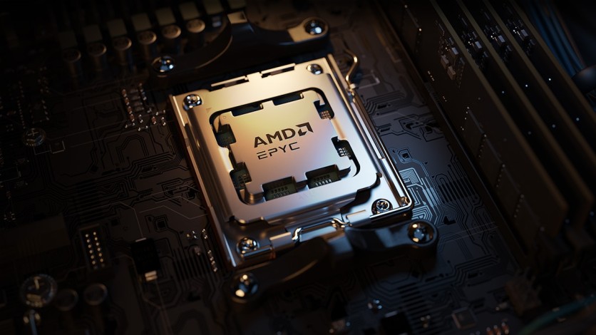
In two days, AMD's EPYC "Venice" server processor — the first high-performance computing chip in the industry to reach production on TSMC's 2-nanometer process node — moves from production ramp to commercial debut at the Advancing AI 2026 conference in San Francisco. That debut carries more than the usual weight of a server CPU launch: Venice lands with a 33% core count increase over its predecessor, a claimed 70% performance advantage, a fundamental redesign of the chip's internal architecture, and a process-node lead over Intel's next P-core Xeon that will last at least through the end of 2027.
For enterprise infrastructure teams, the timing creates a real procurement decision point this week. For the chip industry at large, Venice's production start on TSMC N2 is the first real-world proof that the foundry's new Gate-All-Around nanosheet transistor technology can deliver HPC yields at commercial scale.
What Mark Papermaster Said in Paris: What It Means Wednesday
AMD CTO and Executive VP Mark Papermaster left little room for ambiguity at the RAISE Summit in Paris earlier this month. "We're now on our sixth generation," he said. "So at our Advancing AI event on July 22nd and 23rd, we're rolling out this new generation." No hedging, no conditional language — a direct confirmation from the executive responsible for AMD's architecture roadmap.
That bluntness reflects a product already in volume production rather than one still racing toward tape-out. AMD announced the N2 production ramp in Taiwan in May, marking the first time any company had committed a high-performance computing design to volume output on the node. Future production is also planned at TSMC's Arizona campus, though volume there is not expected before 2028 at the earliest.
TSMC's 2nm Node Introduces Gate-All-Around Transistors: Venice Is First to Deploy Them at HPC Scale
To understand why Venice's node matters as much as its core count, it helps to understand what TSMC's N2 process actually changes at the transistor level. Every prior generation of EPYC — from Naples through Turin — was built on FinFET transistor technology, where a silicon fin protrudes vertically through a gate. At N2, TSMC makes its first commercial deployment of Gate-All-Around (GAA) nanosheet transistors, in which the gate wraps 360 degrees around stacked horizontal sheets of silicon channel material. That geometry gives the gate superior electrostatic control over the channel, reducing leakage and enabling smaller transistors without sacrificing performance.
The practical result, according to TSMC: a 10-15% performance improvement at the same power envelope as the N3E node used in Turin, or a 25-30% power reduction at the same performance level. Transistor density exceeds 310 million transistors per square millimeter, compared to roughly 292 million on TSMC's N3E — a meaningful improvement for a design packing 256 cores into a single socket.
AMD's Venice is the first HPC product anywhere in the industry to enter volume production on this node. Apple reportedly secured the largest share of initial N2 capacity for its consumer silicon; AMD's EPYC is the first product to demonstrate N2 at scale in a thermally demanding, always-on data center context.
How Venice Is Built Differently From Any Prior EPYC
Venice's architecture is not a continuation of Turin's chiplet topology — it is a redesign. Turin, the current Zen 5 flagship, used 16 Core Complex Dies (CCDs) organized around a single large I/O die, with each CCD carrying 12 or 16 CPU cores. Venice cuts that CCD count in half and more than doubles the cores per chiplet.
The flagship Venice package uses eight CCDs, each built on TSMC N2 silicon and carrying 32 Zen 6c cores, flanked by two slender I/O dies built on a 4nm node and mounted at the center of the package. That dual-IOD design replaces the single large IOD that all prior EPYC generations shared. The practical benefits are two-fold: the I/O workload is distributed, reducing the single-die bottleneck at memory and PCIe routing, and the 16 memory channels the two IODs collectively support (vs. 12 for Turin's SP5 platform) enable per-socket bandwidth of up to 1.6 TB/s.
The package itself uses 2.5D advanced packaging rather than the organic substrate connections that linked chips in prior EPYC generations. That shift eliminates the SerDes links between chiplets that were the bandwidth and latency bottleneck in older multi-die designs. Each CCD at roughly 165mm² of N2 silicon carries approximately 128MB of L3 cache (at AMD's documented 4MB-per-core allocation), yielding a potential 1,024MB of L3 across the full socket — by far the largest on-die cache in any x86 server processor.
The platform also moves from PCIe Gen 5 to PCIe Gen 6, doubling the per-lane bandwidth in each direction from 64 GB/s to 128 GB/s. For AI data centers where CPUs must continuously feed data to GPU accelerators, that bandwidth ceiling is the relevant constraint. Venice's PCIe 6 support means the CPU can sustain data movement to attached accelerators at rack scale without becoming the bottleneck in high-throughput inference and training pipelines.
What Venice does not preserve is backward compatibility. The new SP7 socket is incompatible with the SP5 infrastructure Turin runs on, meaning enterprise buyers must plan a complete server platform replacement — not a CPU upgrade — to adopt Venice.
AMD's Lead Against Intel: What the Data Actually Says
AMD already held a record 46.2% of x86 server CPU revenue in the first quarter of 2026, according to Mercury Research — a figure that reflects both EPYC adoption and AMD's structurally higher average selling price. At only 33.2% unit share, AMD generates nearly half of all x86 server CPU spending while shipping roughly one-third of the units — a premium pricing position that Venice is expected to extend.
The competitive timing could not be more favorable for AMD. Intel's Clearwater Forest — the Xeon 6+ E-core processor on the Intel 18A node, with up to 288 cores — is now available, but it targets high-density, scale-out workloads rather than the general-purpose and AI-orchestration segment Venice aims at. Intel's P-core Xeon response — Diamond Rapids — has been officially confirmed for 2027, meaning enterprises choosing between Venice and an Intel P-core server platform will wait at least 12 months for the comparison to be meaningful.
AMD's first-quarter data center revenue reached $5.8 billion, up 57% from the same period a year earlier — and, for the first time, ahead of Intel's data center segment revenue. Venice's commercial launch is the product that AMD expects to sustain and extend that trajectory.
AMD has claimed that a 256-core Venice CPU outperforms Nvidia's Grace CPU in Vera Rubin by 3.3x in rack-level performance. That figure is AMD's own internal benchmark and has not yet been validated by independent third parties. Real-world benchmark results from production systems are among the most closely watched deliverables from this week's event.
Read more: AMD Helios Faces Nvidia Vera Rubin at July 23 Keynote: Memory Leads, Training Trails
Venice Inside Helios: What Wednesday's Launch Actually Delivers
Venice arrives as part of a system, not as a standalone processor. AMD's Helios rack-scale AI platform pairs EPYC Venice CPUs with Instinct MI455X accelerators and Pensando networking hardware into a fully integrated, liquid-cooled double-width rack.
Each Helios rack contains 18 compute trays. Each tray carries four MI455X GPUs and one Venice CPU. At rack scale, that means 72 MI455X accelerators, more than 4,600 EPYC Venice CPU cores, 31 TB of HBM4 memory with 1.4 PB/s aggregate memory bandwidth, and 2.9 FP4 exaflops of AI inference compute. The MI455X itself carries 432 GB of HBM4 per chip across two Graphics Compute Dies and two memory controller dies, with 16 HBM4 memory stacks delivering 19.6 TB/s per chip.
The scale-up interconnect inside a Helios rack uses UALink-over-Ethernet — an open-standard specification backed by a consortium including AMD, Broadcom, Cisco, Google, HPE, Intel, Meta, and Microsoft — rather than Nvidia's proprietary NVLink. On paper, the aggregate intra-rack bandwidth of 260 TB/s is competitive with Nvidia's NVLink72 at 259 TB/s; in practice, the systems use different PHY implementations and any performance comparison awaits independent production benchmarks.
Helios Commits Buyers to AMD's Full Stack: HBM4 Availability Limits the Timeline
The most significant structural fact about Helios that the spec sheet does not communicate is that a Helios customer is not purchasing a component — they are committing to AMD's complete stack. The MI455X's HBM4 memory requires a 2,048-bit routing interposer that is incompatible with HBM3e platforms; customers cannot migrate MI455X cards into Nvidia server infrastructure or vice versa without a full system replacement.
The supply side adds a further constraint that AMD has not prominently foregrounded: all 2026 HBM4 production is reportedly allocated to hyperscalers, with volume beyond engineering samples not expected to reach general availability until 2027 for most buyers. Independent analysis from MLQ AI places mass production of the MI455X itself at Q2 2027. What Venice and Helios enable for the largest cloud and hyperscale customers starting this quarter may remain limited for mid-market enterprise buyers for another 6-12 months.
Enterprise decision-makers evaluating Helios against Nvidia's Vera Rubin NVL72 should also account for the software layer: AMD's ROCm stack, while improving, does not yet match the breadth and depth of Nvidia's CUDA ecosystem for the full range of AI and HPC workloads.
Read more: CES 2026: AMD Details Helios AI Rack and Next-Gen Instinct MI400 GPUs
What Wednesday and Thursday Look Like
AMD's Advancing AI 2026 conference runs July 22–23 at the Moscone Center in San Francisco. Wednesday opens the Expo and includes technical sessions, workshops, and a welcome reception. Thursday begins with Lisa Su's keynote at 9:30 AM PT, followed by tech talks, certifications, breakouts, and a closing reception.
The event features over 100 sessions and a speaker roster that extends well beyond AMD's own executives: confirmed partners on stage include Meta, OpenAI, xAI, Oracle, Microsoft, Cohere, HUMAIN, and Red Hat. In-person registration is full; AMD will stream the keynote on its YouTube channel for remote attendees.
Among the open questions Wednesday's sessions are expected to resolve: precise Venice SKU configurations and core-count tiers across the SP7 and SP8 platform variants, final TDP ranges, and pricing relative to Intel's current Xeon 6 lineup. Lisa Su's keynote on Thursday may also offer a preview of AMD's consumer Zen 6 roadmap, though leaked timelines point consistently to a Ryzen 10000 desktop announcement at CES 2027, with availability in the first half of 2027.
Why Chip Designers Across the Industry Are Watching
Venice's commercial debut is not just AMD's news. As the first HPC product to enter volume production on TSMC N2, Venice will generate the first sustained, real-world yield and thermal data from the node in a demanding 24/7 data center environment. That data — on how GAA nanosheet transistors behave under extended HPC load, at what clock frequencies, and at what thermal margins — is information that Apple, Qualcomm, Nvidia, and Broadcom are each incorporating into their own N2 tapeout planning.
For Intel, the timing remains difficult. The Clearwater Forest E-core Xeon is available, but independent analysis from SemiAnalysis noted it showed only about 17% performance improvement over its predecessor at matched core counts — a result that suggested Intel's 18A foundry process is serving more as a yield-learning vehicle than a competitive performance leap in this generation. Diamond Rapids — the P-core part that would more directly challenge Venice — is not expected until mid-2027 on Intel 18A-P.
Venice's Zen 6 microarchitecture is also a preview of the consumer silicon that will eventually cascade into Ryzen desktops and laptops. The instruction-per-clock improvements, branch predictor refinements, and cache architecture changes AMD encoded into Venice's cores will form the foundation of the Ryzen 10000 lineup — meaning Wednesday's server launch is, for PC builders following AMD's roadmap, their first real look at the performance foundation of their next CPU upgrade.
Frequently Asked Questions
What is AMD EPYC Venice and how is it different from the previous generation?
EPYC Venice is AMD's 6th-generation server processor, based on the Zen 6 architecture and built on TSMC's 2-nanometer process node — the first HPC chip in the industry to reach volume production on that node. Compared to its predecessor EPYC Turin (Zen 5, TSMC N3E), Venice uses eight Core Complex Dies with 32 cores each instead of 16 CCDs with 12-16 cores, bringing the flagship core count to 256 (up 33%). The platform moves to a new SP7 socket supporting 16 memory channels and up to 1.6 TB/s of bandwidth, and adopts PCIe Gen 6 which doubles the per-lane bandwidth available for CPU-to-GPU data movement compared to PCIe 5. The process node change from TSMC N3E to N2 also introduces Gate-All-Around nanosheet transistors for the first time, replacing FinFET technology that has been the industry standard since 2011.
When will Venice systems actually be available to buy, and who can get them first?
AMD expects the first Venice-based systems to ship in Q3 2026. However, a meaningful caveat applies: the HBM4 memory required by the Helios rack platform is reported to be fully allocated to hyperscale customers through 2026, and some independent analysts estimate that MI455X accelerators — the GPU pairing for Helios racks — will not reach mass production until Q2 2027. Enterprise buyers that are not among AMD's major hyperscale partners (Meta, Oracle, OpenAI, and similar) should expect constrained availability through at least early 2027 for full Helios rack deployments. Standalone Venice CPU servers without the Helios GPU pairing may follow a different timeline to be clarified at the event.
If Venice is a platform commitment, what does that actually mean for a buyer evaluating it against Nvidia?
Choosing the Helios rack-scale platform is not equivalent to buying a GPU upgrade — it is a complete infrastructure decision. The MI455X accelerators use HBM4 memory on a 2,048-bit interposer that is physically and electrically incompatible with HBM3e-based Nvidia platforms. A data center that commits to Helios cannot reuse that GPU infrastructure on Nvidia hardware, and vice versa. Additionally, AMD's ROCm software stack, while significantly improved, does not yet match CUDA's coverage of AI frameworks, scientific computing libraries, and third-party tooling — a real operational cost for teams whose existing workflows are CUDA-native. Buyers comparing Helios to Nvidia's Vera Rubin NVL72 are choosing between AMD's higher HBM4 memory capacity (31 TB per Helios rack vs. approximately 20.7 TB for Vera Rubin NVL72) and Nvidia's more mature software ecosystem and established interconnect performance history.
Will Zen 6 come to desktop CPUs, and when?
Yes, but not in 2026. The consumer desktop version of Zen 6 — codenamed "Olympic Ridge" and expected to launch as the Ryzen 10000 series — is pointed toward CES 2027 in January, with a consumer release expected in the first half of 2027. AMD has confirmed that AM5 socket support extends at least through 2029, meaning current B650, X670, and X870 motherboard owners should be able to adopt Ryzen 10000 with a BIOS update and no new motherboard purchase required.

-
 C114 Communication Network
 -
 Communication Home
