

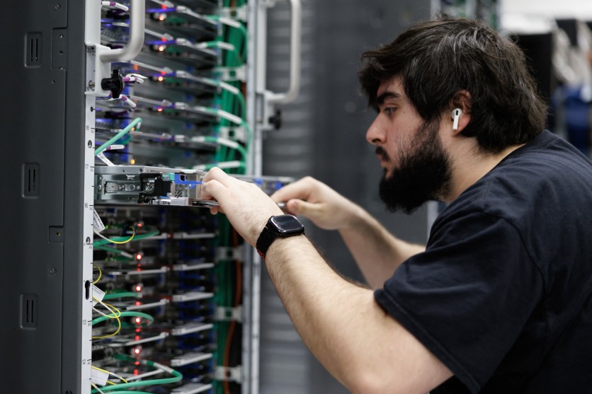
An employee pulls out a server rack shelf at the rear of a Trainium3 UltraServer at an Amazon Web Services QA lab in Austin, Texas, on February 3, 2026. Tech titan Amazon is working to step out of Nvidia's shadow with custom "Trainium" chips designed specially for machine learning as billions of dollars are poured into artificial intelligence (AI). Amazon subsidiary Annapurna Labs in Austin, Texas, was testing the longevity of its latest generation Trainium during a recent visit by AFP to the facility. Texas is emerging as a US tech world El Dorado, luring investments with cheap energy, relaxed regulations, tax incentives and reasonably affordable real estate for massive data centers. Mark Felix/Getty Images
An AI chip startup that spent four years building in near-total silence came out of stealth Tuesday with a set of numbers that are difficult to dismiss: $800 million raised, more than $1 billion in signed customer contracts, a working chip entering production, and an investor list that spans Nobel laureates, deep learning pioneers, and some of the most rigorous allocators in quantitative finance.
The company is Etched, and its core bet is as stark as it is unusual. Its chip, called Sohu, is designed for transformer inference — the ongoing process of running large language models against live queries — and is optimized for that workload at a level of architectural specificity that no GPU can match. The company says first racks ship this summer.
What Etched is claiming is not incremental improvement. It is a claim that the dominant paradigm in AI inference hardware — general-purpose GPUs running CUDA — is structurally inefficient for the workload that now consumes the majority of AI compute spending, and that a purpose-built alternative can deliver an order of magnitude more throughput at lower cost and power. Whether that claim holds up under production conditions is the question that the next year will answer.
Read more: Custom AI Chips Outpace Nvidia GPU Growth in 2026: ASIC Shipments Set to Triple GPU Rate
Inside the Transformer ASIC: How Sohu Closes the FLOP Utilization Gap
The transformer architecture — introduced in the 2017 "Attention Is All You Need" paper — processes text by converting tokens into vectors and contextualizing each against all others in the context window through a multi-head attention mechanism. Every major large language model, from GPT to Llama to Claude, runs transformer attention at the core of every inference request.
On a general-purpose GPU, handling that attention requires loading model weights and a key-value cache from high-bandwidth memory, dispatching a CUDA kernel to perform the attention calculations, and managing thread scheduling across thousands of parallel cores — only some of which are doing useful work at any given time. The result is that GPUs typically achieve 30 to 40 percent of their theoretical FLOP capacity on transformer inference workloads. The remaining compute sits idle.
Etched's production architecture targets that gap through two hardware innovations. The first, which the company calls Low Voltage Inference, runs the chip's math blocks at under half the voltage of conventional AI chips. By lowering operating voltage, Etched increases FLOP density dramatically without triggering the thermal throttling that causes conventional chips to downregulate their clock speeds under sustained load. The company says this allows the cluster to run trillion-parameter sparse models — including mixture-of-experts architectures — at over 80 percent of peak FLOP throughput, a utilization level that general-purpose GPU clusters cannot sustain.
The second innovation, Cluster Scale Memory, creates a shared, low-latency memory pool across chips in the scale-up domain using a proprietary high-bandwidth interconnect. Standard high-bandwidth memory chips struggle with the memory access patterns of the decode phase of inference — where each new token requires reading the full key-value cache — because the bandwidth is shared between weight reads and cache reads. Etched's design separates those paths and adds an ultra-low-latency fabric across chips, addressing both the throughput bottleneck and the per-token latency that makes high-batch serving feel sluggish.
The chip is manufactured on Taiwan Semiconductor Manufacturing Company's N4P process — a specific 4nm-generation process node — and pairs the compute die with 144 gigabytes of HBM3E memory. An eight-chip server can hold a 400- to 600-billion parameter model with tensor parallelism. For pure throughput on dense transformer models, Etched says one eight-chip server can process more than 500,000 tokens per second running Llama 70B, against roughly 23,000 tokens per second for an equivalent eight-GPU H100 server and roughly 43,000 to 45,000 for a B200 server.
Those figures come from Etched's own published materials. As of Tuesday's stealth exit, no third-party benchmark organization has published independent throughput measurements from physical Sohu hardware under production conditions.
The Investors: What $800M and $1B in Orders Signal
Etched has raised $800 million across multiple financing rounds. The latest, a $500 million round that closed in December 2025, set a $5 billion post-money valuation and was led by Stripes. It included a strategic investment from VentureTech Alliance — a fund with ties to Taiwan Semiconductor Manufacturing Company — alongside Peter Thiel, Jane Street, Hudson River Trading, Jump Trading, Two Sigma, Ribbit Capital, and additional firms. Jane Street led a previously unannounced round and has invested more than $100 million in Etched in total, according to Bloomberg.
The angel list adds a different kind of credibility. Geoffrey Hinton, the Nobel Prize–winning deep learning researcher who first demonstrated that neural networks could learn useful representations; Fei-Fei Li, the Stanford AI researcher whose ImageNet project catalyzed the computer vision revolution; Andrej Karpathy, who led Tesla's Autopilot AI program before joining Anthropic; and macro investor Stanley Druckenmiller are all backing the same chip.
That breadth matters. Theoretical AI researchers, applied ML practitioners who have built and deployed real inference systems at scale, and allocators who make their living on precision bets — if this group has collectively decided the Etched thesis is credible, the thesis has survived some of the most demanding scrutiny available in the field.
The VentureTech Alliance investment is worth noting separately. Because the fund has ties to TSMC, its participation suggests a manufacturing relationship that goes beyond a standard customer agreement and may include priority access to N4P capacity as Etched ramps production. Etched says it has opened a Taiwan factory and data center specifically to support the ramp.
Read more: OpenAI's First Custom AI Chip Targets 50% Cheaper Inference: Jalapeño Unveiled
Why Nvidia Would Not Make This Chip
Nvidia's competitive moat in AI hardware is not primarily its silicon. It is CUDA — a programming model and library ecosystem accumulated over roughly two decades. The cuDNN and cuBLAS libraries that PyTorch and TensorFlow depend on, the FlashAttention and PagedAttention optimizations built into production inference stacks, the TensorRT compiler that powers enterprise deployments — all of this is CUDA-native and requires a full stack rewrite to move off GPU hardware. Switching to Etched means rebuilding a production inference environment using the company's proprietary compiler, with no CUDA, vLLM, or TensorRT compatibility.
Nvidia could in principle build a highly optimized inference accelerator. The structural reason it likely will not give up its generalism is that CUDA's moat depends on GPUs remaining broadly programmable. A transformer-specialized chip from Nvidia would be a concession that general-purpose flexibility is no longer worth paying for — which would accelerate the CUDA ecosystem's own obsolescence. That constraint is precisely what Etched is betting on. If the inference era is durable and large enough, Nvidia's generalism becomes a structural tax rather than a feature, and Nvidia is economically incentivized to maintain it.
Etched CEO Gavin Uberti has framed the company's position in binary terms: if the transformer architecture endures at scale, Etched has the potential to become an extraordinarily large business. If it does not, the chips become expensive paperweights. That candor about the downside is itself a signal — it suggests the company has thought carefully about what it is betting on, rather than hedging.
What Is Still Unverified and What Has Already Shipped
The $1 billion in signed customer contracts represents committed purchase orders, not deployed systems or recognized revenue. Etched says it has been testing racks with customers and running production traffic patterns through its simulator, and that "early customer tests show us achieving state-of-the-art throughput, latency, and power efficiency on inference workloads." The company has not released specific numbers from those tests.
Performance claims — one server replacing 160 H100 GPUs, 500,000 tokens per second on Llama 70B, 80 percent peak FLOP utilization on sparse MoE models — are all self-reported from Etched's published materials. The benchmark conditions that produce the headline throughput figure (2,048 input tokens, 128 output tokens, high batch throughput rather than single-request latency) are conditions Etched's architecture is optimized for. Real production workloads involve more variable context lengths and batch distributions, which will produce different results. At high batch sizes, a single H100 can produce roughly 45,000 tokens per second — a narrower gap than the headline comparison to the 23,000-token low-batch figure suggests.
The architectural risk is real and worth stating plainly. Etched's chips are not the original Sohu design that could run only dense transformer models. The production architecture the company is shipping claims to handle mixture-of-experts models and long-context workloads. But until independent benchmarks confirm that those capabilities perform as described under production conditions, the full scope of the chip's workload compatibility remains company-claimed rather than independently demonstrated.
The analogy the company's founders invoke frequently is bitcoin mining. Specialized mining ASICs displaced GPU mining because they were 13 times faster on the specific SHA-256 computation miners needed — and once they arrived, GPU mining became obsolete within months. Etched's argument is that the same logic applies to transformer inference: if a purpose-built architecture is substantially more efficient on the dominant AI workload, economic pressure will drive adoption. The difference is that SHA-256 is one fixed calculation, while transformer inference is a family of workloads whose characteristics vary in ways that matter for hardware design. Whether the analogy holds depends on how stable the inference workload profile turns out to be across the architectures customers actually deploy.
Etched has made the most credible opening move yet seen against Nvidia's inference business: a working chip, a manufacturing partnership with the world's leading foundry, $800 million to execute on it, and a billion dollars in orders that suggest serious buyers have done the calculation and decided the risk is worth taking. The production proof will arrive over the next six to twelve months. Until then, the claim is the credible hypothesis, not the confirmed result.
Frequently Asked Questions
What is the Etched Sohu chip, and how does it differ from a GPU?
Sohu is an AI inference accelerator built around two proprietary architectural innovations: Low Voltage Inference, which runs the chip's math blocks at below-half the voltage of conventional AI chips to maximize FLOP density without thermal throttling; and Cluster Scale Memory, which creates a shared low-latency memory pool across chips to eliminate the bandwidth contention between weight reads and key-value cache reads that constrains GPU inference performance. Unlike a GPU, which uses a general-purpose programming model to run any workload, Sohu hard-codes the transformer computation graph into silicon to eliminate the instruction-scheduling and kernel-launch overhead that causes GPU FLOP utilization to fall to 30 to 40 percent on inference workloads.
Can Sohu replace Nvidia GPUs for AI inference?
For transformer inference workloads — including, the company now claims, sparse mixture-of-experts models and long-context serving — Etched's production chip targets a significant throughput and cost advantage over GPU clusters. The switching cost is substantial: moving to Sohu requires rebuilding a production inference stack using Etched's proprietary compiler, with no compatibility with CUDA, vLLM, or TensorRT-LLM. No independent benchmark has verified Etched's throughput claims under production conditions. The company plans to begin shipping racks to customers this summer, which is when real-world performance data will begin to emerge.
What are the architectural risks of Etched's transformer-focused design?
The production chip claims to handle mixture-of-experts models and long-context workloads in addition to dense transformer inference — a capability the original Sohu design announcement did not include. Whether the production chip delivers on those claims at the performance levels Etched describes, and whether it serves the full range of models that enterprise inference customers actually deploy, will be answered by independent benchmarks from production deployments. The broader architectural risk is evolution: if frontier models continue shifting toward hybrid architectures that combine transformer attention with state-space model components or other mechanisms, the degree to which fixed-function silicon can accommodate those changes without a hardware revision is a genuine open question.
Who backed Etched, and has the chip been independently tested?
Investors include Stripes, Jane Street, Peter Thiel, Hudson River Trading, Jump Trading, Two Sigma, VentureTech Alliance, and Ribbit Capital, alongside angel investors including Geoffrey Hinton, Fei-Fei Li, Andrej Karpathy, and Stanley Druckenmiller. As of Tuesday's stealth exit, the chip has been demonstrated to investors and early customers but has not been publicly benchmarked by an independent third party. Etched's A0 silicon has returned from TSMC's N4P process and is in customer validation. Independent performance data is expected to follow as production racks ship this summer.
-
 C114 Communication Network
 -
 Communication Home
