
 Search

Amd.com
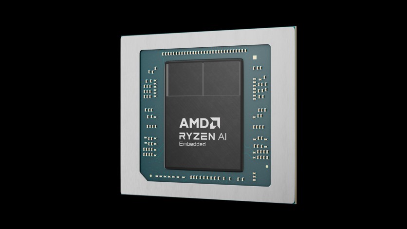
AMD has formally launched the Ryzen AI Embedded X100 Series processors for physical-AI robotics and industrial systems, bringing the same Strix Halo processor silicon that powers the company's Ryzen AI Max consumer chips into ruggedized, production-grade packages with a 10-year supply guarantee and an operating temperature range spanning −40°C (−40°F) to 105°C (221°F). The announcement came Thursday at AMD's Advancing AI 2026 conference at Moscone West in San Francisco, where CEO Dr. Lisa Su formally unveiled the X100 family alongside EPYC Venice server CPUs and the Instinct MI455X GPU accelerator — AMD's most comprehensive AI portfolio launch to date.
For system integrators choosing embedded compute for robots and autonomous systems, the X100 makes a concrete offer that prior generations of x86 chips could not: up to 128 GB of unified memory accessible simultaneously by the CPU, GPU, and NPU from a single coherent pool — a configuration that matters specifically because the vision-language-action models now running in production-level humanoid robots are too large for the VRAM ceilings of conventional embedded GPU designs, and too latency-sensitive to survive the memory copy overhead those designs impose. AMD's Kria AI Robotics Developer Platform claims sub-100 millisecond VLA reasoning latency as a direct result of this architecture.
Six Chips, One Architecture: The X100 Lineup
The X100 family launched with six processor models, all derived from the Strix Halo die that AMD first introduced in consumer form as the Ryzen AI Max+ 395. The three standard models are the X199, X188, and X168; each has an industrial-temperature "i" variant qualified for the full −40°C to 105°C junction range, while standard models are rated from 0°C.
The flagship X199 carries 16 Zen 5 CPU cores and 40 RDNA 3.5 compute units (CUs), delivering AMD's largest integrated GPU configuration in embedded silicon. The mid-tier X188 steps down to 12 CPU cores and 32 CUs. The entry X168 drops to eight cores but retains the 32-CU GPU — preserving GPU compute capacity for workloads where graphics throughput matters more than CPU thread count, as confirmed by VideoCardz in its coverage of the launch.
Every chip in the family includes an XDNA 2 neural processing unit (NPU) rated at up to 50 tera-operations per second (TOPS) of AI inference throughput. Configurable thermal design power spans 45 W to 120 W, and a boost clock of up to 5.1 GHz is available across the range, as detailed by Tom's Hardware in its chip lineup coverage.
All chips share access to up to 128 GB of LPDDR5X-8533 unified memory — a single coherent pool that the CPU, GPU, and NPU read and write without the explicit software-managed copy operations that systems with separate CPU and GPU memory require.
Why 128 GB of Unified Memory Is the Robotics Inference Bottleneck Answer
Vision-language-action (VLA) models are the emerging software architecture for general-purpose robotic control. They take a camera feed, a natural language instruction, and sensor data as input, then output motor commands — replacing the separate perception and control pipelines that older robot software required. The models that perform well on manipulation and navigation tasks are large: OpenVLA, a widely cited benchmark architecture, has more than 7 billion parameters and requires approximately 14 GB of GPU memory at FP16 precision. The EdgeVLA research paper highlights that these systems achieve inference speeds of only 5 to 10 Hz with stationary compute systems — a hard constraint for deployed robots.
The problem is inference speed. OpenVLA runs at about 6 Hz even with an Nvidia RTX 4090 GPU, as noted in the HyperVLA paper on efficient VLA inference. Robotic manipulation typically requires 10 to 30 Hz minimum for responsive grasping and obstacle avoidance. Reducing model precision to meet latency targets degrades task performance.
The architectural path around this constraint is keeping the model's full weight tensor resident in fast, unified memory so that each inference cycle reads from local on-package memory rather than staging through a separate memory fabric. The X100's unified pool addresses this directly: the NPU and GPU share the same 128 GB LPDDR5X pool with the CPU, so an 8-billion-parameter model can remain fully resident during inference without paging or inter-subsystem transfer. AMD's Kria AI Robotics Developer Platform claims sub-100 millisecond VLA reasoning latency as a result.
The unified memory pool also eliminates a per-inference tax that is invisible in benchmark slides but measurable in production: each time a conventional embedded system transfers data from system RAM to GPU VRAM for inference and back, it burns time and power proportional to the data size. For a VLA model running at 20 Hz, that transfer overhead compounds into a meaningful fraction of total power budget. Unified memory architecture removes the transfer entirely.
For context, Apple's M-series chips use the same unified memory concept but implement it with LPDDR5X at up to 614 GB/s bandwidth in the M5 Max, as documented on the Apple M5 Wikipedia page. The X100's LPDDR5X-8533 implementation delivers approximately 135 GB/s — lower bandwidth than high-end consumer implementations, but within a 45–120W industrial power envelope and a 120mm × 120mm (4.7 in × 4.7 in) COM-HPC module footprint that fits into robot chassis designs where Apple silicon was never an option, per the PICMG COM-HPC specification.
Kria SOM and the Turnkey Robotics Platform
Beyond the silicon, AMD is offering two delivery vehicles for the X100. The first is the Kria AI System-on-Module (SOM), a COM-HPC-compliant module that gives system integrators a standardized carrier-board design path. The COM-HPC standard, maintained by the PCI Industrial Computer Manufacturers Group (PICMG) and ratified in 2021, defines a multi-supplier ecosystem of 120mm × 120mm (4.7 in × 4.7 in) modules with 800-pin dual-connector interfaces supporting PCIe Gen 4/5, USB4, and 25 GbE. Carrier boards designed for one COM-HPC module are forward-compatible with future-generation modules from any compliant vendor — a practical advantage for industrial buyers who design custom hardware for 10-year deployment cycles.
The second delivery vehicle is the Kria AI Robotics Developer Platform, which pairs the Kria SOM with AMD's Spartan UltraScale+ FPGA baseboard, providing connectivity for cameras, industrial networking, motor controllers, and robotic sensors. AMD describes the design philosophy for physical AI systems using a body-metaphor hierarchy: the X100 Kria SOM serves as the robot's brain, Versal AI Edge Gen 2 acts as the spine, Zynq UltraScale+ handles joints and motion control, and Spartan UltraScale+ manages sensors. SOM availability from launch partners — Arbor, Congatec, iBase, IEI, Sapphire, and Seavo — is expected in Q4 2026, as CNX Software reported.
Read more: AMD Carries x86 Into Robotics and Cars With Ryzen AI Embedded, Challenging Arm-Based Rivals
How AMD's Benchmarks Were Built, and What to Read Into Them
AMD released two sets of performance comparisons at Advancing AI 2026, and both carry methodology footnotes that matter for how much weight to assign the headline numbers.
In the comparison against Intel's Core Ultra X7 358H — a 16-core Panther Lake chip with a 12-CU Arc integrated GPU — AMD claims a 1.2× to 1.3× lead in GeekBench 6.1 and PassMark, a 1.5× advantage in an unofficial SPECrate 2017 integer run, and graphics margins of 1.4× in Vulkan and 1.7× in OpenGL via GFXBench 5.0, per AMD's newsroom benchmark disclosures. The AI inference numbers are more striking: AMD claims a 1.4× improvement in time-to-first-token and a 3.5× increase in tokens per second running Llama-bench at 45 W.
The caveat on both sides is significant. AMD's X199 was represented not by production X100 hardware but by a Ryzen AI Max+ 395 "configured to reflect Ryzen AI Embedded X199 specifications" running on a Maple reference board. Intel's Core Ultra X7 358H was tested in an MSI Prestige 16 Flip AI+ notebook at a 30 W TDP cap, and AMD then projected 45 W performance for that chip using "publicly available benchmark scaling factors" rather than direct measurement, as Tom's Hardware noted in its coverage of the launch methodology. Neither side of that comparison used the final production hardware buyers will receive.
The Nvidia comparison is similarly structured. AMD's Kria AI Robotics Developer Platform performance claims — including a 3.4× improvement in real-time reliability over the Nvidia Jetson Thor T5000, 2.3× more concurrent agents, and 1.6× more available CPU cores — were generated by AMD partners Open Navigation and mimik, with the AMD side represented by a GMKtech EVO-X2 mini PC running the Ryzen AI Max+ 395 rather than an actual Kria board, as confirmed in the AMD Kria newsroom benchmark footnotes. These comparisons are directionally useful, but independent third-party validation against production X100 hardware remains pending until the chips begin shipping later this year.
AMD's Case Against Nvidia Jetson AGX Thor
Nvidia's Jetson AGX Thor is the established platform in this market segment. The Thor delivers 2,070 FP4 TOPS of AI compute from a Blackwell-architecture GPU with 2,560 CUDA cores and 96 fifth-generation Tensor Cores, running within a 40–130 W power envelope on 128 GB of LPDDR5X memory, per the Nvidia Jetson Thor product page. Confirmed Jetson Thor customers include Amazon Robotics, Boston Dynamics, Figure, and Agility Robotics, as the Nvidia developer blog documents. The platform integrates with Nvidia's Isaac robotics software stack and GR00T foundation models, giving developers a vertically integrated path from foundation model to deployed robot.
AMD's pitch against this incumbent rests on the x86 architecture advantage. The Jetson Thor uses a 14-core ARM Neoverse V3AE CPU — a capable design for robotics control, but one that requires developers to compile, port, or abandon the x86-native tools their teams likely already use. AMD argues that existing Linux toolchains, Python environments, and compiled binaries that run on x86 servers run on the X100 with no modification, narrowing the gap between development environment and production deployment, per the AMD Advancing AI 2026 press release.
The CUDA migration argument is more nuanced. AMD's HIPIFY tool can automate translation of CUDA source code to AMD's HIP C++ portable runtime, and AMD cites approximately 75% code-preservation coverage for this process. AMD's own official HIPIFY documentation qualifies this: the tool "does not automatically convert all CUDA code into HIP code seamlessly," and CUDA libraries without HIP equivalents — including third-party acceleration libraries — cannot be translated automatically. Complex production applications with custom CUDA kernels may require significant manual porting effort beyond what the automation percentage implies.
In raw AI compute, the gap between 2,070 FP4 TOPS (Jetson Thor) and the X100's 50 TOPS NPU is not a direct comparison: the Jetson figure reflects the full Blackwell GPU's AI throughput, while AMD's 50 TOPS figure covers only the dedicated NPU, with the GPU's contribution to inference workloads reported separately through benchmark claims. The X100 is designed for a different performance tier — integrated x86 SoC performance rather than discrete GPU-class throughput — and its competitive argument is total platform value: x86 ecosystem, 128 GB unified memory, and industrial-grade packaging, rather than raw AI TOPS.
AMD vs. Intel Panther Lake: Choosing a Lane
Intel's Core Ultra Series 3, launched at CES 2026 and built on the Intel 18A (1.8 nanometer class) process node, is the more direct technical competitor for the X100. Intel claims up to 180 TOPS of combined AI performance — 120 TOPS from the GPU and 50 TOPS from the NPU — and has specifically certified select Series 3 processors for embedded and industrial use cases, including robotics, smart cities, and healthcare, marking the first time Intel has qualified a client-tier chip for industrial edge deployment. Intel also announced a Physical AI OpenVINO software framework at Computex 2026 targeting robots, drones, and autonomous machines.
AMD's claim of 2.1× higher multithreaded performance and 3.5× higher token generation throughput against Panther Lake comes from the proxy-hardware test described above. The more verifiable differentiator is physical configuration: the X100's 40-CU RDNA 3.5 GPU substantially outweighs Intel's 12-CU Arc integrated GPU in compute units, and AMD's 128 GB unified memory ceiling is significantly higher than the memory configurations that Panther Lake's target power envelope accommodates.
Intel's case is that its unified CPU-GPU-NPU approach reduces total cost of ownership compared to multi-chip robotics compute stacks, and that the Physical AI OpenVINO framework provides a mature software path for robotics developers. Whether the 180 TOPS combined figure or AMD's per-subsystem NPU count is the more meaningful metric depends on the specific inference workload: combined TOPS figures weight GPU throughput heavily, while NPU TOPS figures reflect always-on low-power inference efficiency.
Read more: AMD Advancing AI 2026 Opens With Zen 6 Venice, Helios, and Open AI Rack Bet
What Existing Nvidia Jetson Developers Must Actually Port
The x86 compatibility argument is strongest for CPU-level robot control code — ROS 2 nodes, motion planning algorithms, sensor fusion pipelines written in standard C++ or Python. Those compile and run natively on the X100's Zen 5 cores without modification, and AMD's ROCm open-source GPU software stack supports PyTorch, TensorFlow, and ONNX Runtime for GPU-accelerated inference.
The argument is weaker for developers with deep CUDA investment. HIPIFY handles standard runtime API calls — memory allocation, kernel launch syntax, and most built-in functions — but cannot translate CUDA libraries that lack HIP equivalents, and AMD's own HIPIFY documentation notes that code optimized for Nvidia GPU microarchitecture "might require additional rework to optimize performance on AMD GPUs" after translation. Developers running production inference through Nvidia TensorRT-LLM or FlashAttention 3 — two CUDA-specific acceleration libraries with no full ROCm equivalents as of July 2026 — face more significant porting work.
For new robotics development starting on a clean codebase, the x86 familiarity argument is substantive. For teams migrating active CUDA-based inference pipelines from Jetson, the path requires evaluation of specific library dependencies before committing to the platform.
Does This Actually Challenge Nvidia's Embedded Robotics Moat?
AMD's X100 enters a segment where Nvidia has spent several years building what amounts to a complete vertical stack: the Isaac platform provides the robotics SDK, Holoscan handles sensor processing, GR00T delivers foundation model weights pre-optimized for Jetson hardware, and NeMo provides the pipeline for fine-tuning those models for specific robot deployments. Amazon Robotics, Boston Dynamics, Figure, and Agility Robotics have all committed to Jetson Thor, carrying production deployments into 2026 and beyond.
AMD's counter-move is to reframe the platform choice as an architecture question, not a software question. The argument is that robotic systems integrators who have spent a decade building x86-native control infrastructure — PLCs, motion controllers, RTOS implementations, industrial networking stacks — face less integration friction bringing an x86 SoC into the robot brain than adopting an ARM-based platform that requires rebuilding those interfaces. AMD's 7,000 embedded customers worldwide, as previously reported by TechTimes, represent a customer base for whom this argument is not theoretical.
The 10-year lifecycle guarantee addresses the other half of the industrial buyer's decision: embedded deployments are not consumer cycles. A robot on a factory floor may run the same hardware for a decade, and component availability guarantees matter more to that buyer than benchmark leaderboard position. The X100's supply commitment through at least 2037, as documented by CNX Software, is a commercial differentiator that Nvidia's Jetson platform — which follows roughly a three-to-four-year generational cadence — does not typically match.
The practical answer to whether AMD can challenge Nvidia's embedded robotics position will come from design wins in 2027 and 2028, once production hardware ships and integrators have had time to evaluate the platform against live workloads.
What Comes Next
Customer sampling of the X100 began in June 2026. Production availability, including SOM offerings from Arbor, Congatec, iBase, IEI, Sapphire, and Seavo, is expected in Q4 2026, per AMD's Advancing AI 2026 announcement. Early access to the Kria AI Robotics Developer Platform is open now for qualified customers.
The COM-HPC form factor ensures compatibility with a broad range of existing carrier-board designs, lowering the barrier to platform evaluation for system integrators who already use COM Express or COM-HPC infrastructure. AMD's expanded robotics partner network — including MulticoreWare, mimik, Open Navigation, Kontron, congatec, and MassRobotics — provides software tooling and ecosystem support to match, per the AMD robotics partner network announcement.
The months between now and general production availability in Q4 2026 will be the window in which AMD must demonstrate that the early-access Kria platform can deliver its benchmark claims on final hardware — because proxy-hardware slides and production-silicon performance have historically diverged enough to matter, and Nvidia and Intel will both be watching those numbers closely.
Frequently Asked Questions
What is the AMD Ryzen AI Embedded X100, and how is it different from the consumer Ryzen AI Max?
The X100 is AMD's industrial-grade version of the Strix Halo processor silicon that powers the consumer Ryzen AI Max+ 395 processors. The core architecture — Zen 5 CPU cores, RDNA 3.5 GPU compute units, XDNA 2 NPU, and up to 128 GB unified LPDDR5X memory — is the same. What changes for the embedded version is the qualification envelope: the X100 is rated for −40°C (−40°F) to 105°C (221°F) continuous operation, ships in a ruggedized BGA (ball grid array) package designed for vibration and thermal stress, and carries a 10-year supply guarantee (availability through at least 2037) that consumer parts do not offer, as detailed on the AMD Ryzen AI Embedded X100 product page.
Why does 128 GB of unified memory matter specifically for robotics, and does the X100 actually match what Nvidia Jetson Thor offers?
The unified memory matters because vision-language-action (VLA) models — the AI architecture that lets robots interpret camera feeds and language instructions to output motor commands — are large enough that keeping them resident in fast on-package memory makes the difference between inference at 6 Hz (not fast enough for responsive manipulation) and inference at real-time robotics rates, as documented in the EdgeVLA efficiency research. The Jetson AGX Thor also offers 128 GB of LPDDR5X memory, per the Nvidia Jetson Thor specifications, so the ceiling is matched. What differs is architecture: the X100 is an x86 APU with a unified coherent pool; the Jetson Thor uses an ARM CPU architecture with CUDA-accelerated GPU inference that delivers significantly higher raw AI TOPS (2,070 FP4 versus the X100 NPU's 50 TOPS) but requires Nvidia's proprietary software stack to unlock.
When can system integrators actually buy and build with the AMD X100?
Customer sampling began in June 2026. Production availability for COM-HPC system-on-modules from launch partners (Arbor, Congatec, iBase, IEI, Sapphire, Seavo) is expected in Q4 2026, with early access to the Kria AI Robotics Developer Platform already open, as confirmed in the AMD Kria developer platform announcement. Independent validation of the X100's benchmark claims using production hardware — rather than the configured consumer silicon AMD used in its Advancing AI 2026 comparisons — will be available once the chips ship.
Does migrating existing Nvidia CUDA code to AMD's platform actually work, and how much effort does it take?
AMD's HIPIFY tool automates translation of standard CUDA runtime API calls, kernel launch syntax, and most built-in functions to AMD's HIP C++ portable runtime, and AMD cites approximately 75% code-preservation coverage for this process. However, CUDA libraries without HIP equivalents — including frameworks like TensorRT-LLM and FlashAttention 3 — cannot be translated automatically, and AMD's own HIPIFY documentation states that code optimized for Nvidia GPU microarchitecture may require additional manual rework to reach equivalent performance on AMD hardware. For teams starting new robotics development on x86-native code, the transition is straightforward. For teams with deep CUDA library dependencies, the porting effort requires workload-by-workload evaluation before committing to the platform.

-
 C114 Communication Network
 -
 Communication Home
