
 Search

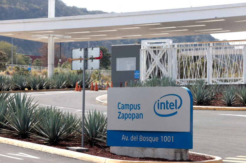
View of the U.S. Intel company building in Zapopan, Jalisco state, Mexico, taken on January 24, 2025. (Photo by ULISES RUIZ / AFP) ULISES RUIZ/AFP via Getty Images
Intel's 18A manufacturing node has crossed the commercial viability threshold that analysts have long used as the benchmark for serious foundry competition: roughly 85% yield on a leading-edge process. That milestone, reported Tuesday by KeyBanc Capital Markets, arrived alongside an independent validation from ASML that gives the figure considerably more weight — the Dutch lithography giant confirmed that Intel Foundry has become the first company in the industry to ship a high-volume logic product using High NA EUV lithography, deployed on Panther Lake processors currently shipping to customers.
The convergence of those two developments in a single morning also surfaced a less-discussed story that may matter even more to the artificial intelligence supply chain: Intel's EMIB-T advanced packaging technology has reached 98% yield, matching the performance level of TSMC's CoWoS — the packaging format that integrates AI accelerators with High Bandwidth Memory and whose chronic supply shortage has been the single most binding constraint on how fast hyperscalers can deploy AI infrastructure. For the first time, chip designers have a commercially viable, U.S.-based alternative to CoWoS operating at comparable quality levels, according to Intel EMIB-T yield data from KeyBanc's supply-chain checks.
85% Yield Is Where Foundry Economics Change
In semiconductor manufacturing, yield — the percentage of chips on a wafer that pass quality inspection — is the primary determinant of whether a process node can sustain commercial production. The basic economic relationship is direct: cost per chip equals wafer cost divided by (yield × dies per wafer). When yield is low, that denominator collapses, making each good chip prohibitively expensive regardless of how sophisticated the technology is.
Industry sources have historically pegged ~85% as the practical floor for a process node to compete in the merchant foundry market. Below that threshold, a node can demonstrate technical capability but struggles to support the economics that external customers — who depend on consistent, high-volume supply at predictable cost — require before committing designs. Above it, cost per chip normalizes rapidly, and the node becomes a sustainable revenue platform.
Intel's 18A node, which entered high-volume manufacturing in late 2025, now sits at approximately 85% yield, up from roughly 65% in the prior quarter — a jump of around 20 percentage points in a single quarter. That pace is consistent with what Intel CEO Lip-Bu Tan described as the industry standard of 7 to 8 percent yield improvement per month, and it confirms the ramp that Tan said Intel was achieving after deploying best practices with ecosystem partners, as TrendForce reported in May 2026 citing CNBC.
For context: per the same KeyBanc supply-chain data, TSMC's competing N2 node sits at approximately 90% yield, leaving Intel about five percentage points behind the market leader. Samsung Foundry's SF2 node — Intel's other primary competitor in the 2nm-class tier — remains at 50% to 60%, leaving it far from commercial scale for merchant customers, as detailed in KeyBanc's yield comparison data.
KeyBanc analyst John Vinh, whose research note drove Tuesday's market reaction, framed the improvement concisely: yields are changing the story. The firm raised its Intel price target from $110 to $155, maintaining an Overweight rating, and introduced long-range 2030 revenue and earnings estimates of $132 billion and $7.58 per share, with foundry operations accounting for $10.6 billion of that total and EMIB-T packaging accounting for more than $22 billion, per Vinh's full 2030 model as reported by Investing.com.
What Makes Intel 18A Technically Distinct
Not all 85%-yield nodes are the same, and Intel 18A's architecture gives it specific advantages that matter for the AI and high-performance computing workloads at the center of the current industry buildout.
The node combines two innovations that are each debuts in high-volume production. The first is RibbonFET, Intel's gate-all-around transistor design, in which the channel is fully surrounded by the gate rather than touched on three sides as in the older FinFET architecture. Full gate enclosure allows more precise control of current flow, reduces short-channel effects that cause power leakage at small dimensions, and enables higher drive current from a smaller footprint. The second is PowerVia, Intel's backside power delivery network — the industry's first implementation at production scale. Traditional chip designs route both power and signal wires through the same front-side metal layers, creating congestion that limits routing density and causes voltage drop under load. PowerVia moves power delivery to the wafer's backside via through-silicon vias, freeing the front side entirely for signal routing. The result, per Intel's measurements and partially corroborated by independent analyst TechInsights: approximately 30 percent reduction in voltage droop and up to 40 percent improvement in peak turbo frequency capability versus FinFET designs, as Tom's Hardware's technical comparison of 18A and TSMC N2 documents.
The combination gives 18A a specific advantage in raw performance relative to its 2nm-class peers. TechInsights' independent analysis ranks Intel 18A highest in performance among 2nm-class nodes — scoring 2.53 on its custom scale versus 2.27 for TSMC N2 and 2.19 for Samsung SF2, as TechPowerUp reported citing the TechInsights research. TSMC N2's countervailing advantage is transistor density: at roughly 313 million transistors per square millimeter in high-density standard cells, it significantly exceeds 18A's 238 million per square millimeter. For workloads where layout compactness and per-transistor cost matter most, TSMC N2 holds an edge. For workloads where high-frequency performance and power efficiency per compute operation matter most — the dominant AI training and inference profile — 18A's architecture provides structural advantages that are increasingly relevant to the customer conversations Intel is having.
Read more: Chip Supply Shifts From TSMC: Google's Reported Intel TPU Order Lifts Foundry, but Doubts Remain
ASML Makes Intel the Industry's First High NA EUV Production Site
The technical credibility of Tuesday's milestone rests in part on its independent confirmation. ASML — the Dutch lithography company whose machines are the only commercially available tools capable of printing patterns at leading-edge dimensions — issued a formal press release Tuesday morning confirming that Intel Foundry has entered high-volume manufacturing for a subset of its Panther Lake (Core Ultra Series 3) processors using ASML's EXE High NA EUV lithography technology, making Intel the first company in the industry to ship a high-volume logic product produced this way.
High NA EUV operates at a numerical aperture of 0.55, compared to 0.33 in standard EUV (the NXE series that ASML has supplied since the early 2020s). The difference follows the Rayleigh criterion governing optical resolution: resolution scales inversely with numerical aperture, so increasing NA from 0.33 to 0.55 delivers a roughly 67% improvement in achievable resolution. In practical manufacturing terms, this enables patterning of finer features with fewer multi-patterning passes, reducing process complexity and improving edge placement accuracy — factors that become critical as nodes push toward 1nm-class dimensions.
For Intel's 18A node specifically, ASML's announcement clarified that specific layers of the 18A stack are now dual-qualified on High NA EUV in Oregon, with product already shipping at yields matched to the existing NXE EUV platform. This is not a wholesale transition of 18A to High NA EUV — it is a qualification step that gives Intel production data, uptime measurements, overlay accuracy benchmarks, and manufacturing implementation experience that will prove essential for its next node, 14A, which is designed from inception to use High NA EUV extensively.
The significance of the timing gap is considerable. TSMC is not expected to deploy High NA EUV in production until approximately 2029, as TrendForce's coverage of TSMC's technology roadmap through 2029 confirms. Intel's 18-to-24-month head start in production-level High NA EUV experience represents a manufacturing learning advantage that compounds over time: the data Intel is accumulating on tool behavior, resist performance, and defect mechanisms at production volumes gives its 14A node a running start that TSMC's equivalent node will not have when it deploys the same tools.
ASML President and CEO Christophe Fouquet described the milestone as a substantial development in semiconductor lithography, noting that the increased resolution and better process control made possible by High NA EUV open the path toward broader industry adoption of the technology. Intel EVP and General Manager Naga Chandrasekaran framed the achievement as validation that High NA EUV can be integrated into advanced semiconductor manufacturing at scale, while providing customers with increased output from the existing tool fleet during the transition, per the ASML press release's executive quotes.
EMIB-T at 98% Yield Breaks AI Builders' Sole Dependence on TSMC CoWoS
The packaging side of Tuesday's story deserves equal attention, because it addresses a supply-chain problem that has constrained AI infrastructure buildout more severely than wafer supply shortages.
TSMC's CoWoS — Chip-on-Wafer-on-Substrate — is the advanced packaging technology that places AI accelerator dies alongside stacks of High Bandwidth Memory on a silicon interposer, connecting them with the dense, short interconnects that enable memory bandwidth in the terabytes-per-second range. Without CoWoS-level packaging, large AI accelerators cannot be built at the density and bandwidth required for modern model training. And CoWoS is produced almost exclusively at TSMC — it is a captive technology, available in limited quantities, with lead times exceeding a year and demand that has outrun every capacity expansion TSMC has attempted since 2023, as analysis of AI chip packaging constraints documents.
Intel's EMIB-T — Embedded Multi-die Interconnect Bridge with Through-Silicon Vias — is a structurally different approach to the same problem. Where CoWoS-S covers the entire package footprint with a silicon interposer, EMIB-T embeds small silicon bridges into an organic substrate at exactly the die-to-die interfaces where high-density routing is needed, leaving the rest of the substrate to standard organic routing. The EMIB-T variant adds through-silicon vias to the bridges, enabling vertical power and signal routing compatible with HBM4 and HBM4e memory at 12+ gigabits per second. The architecture achieves approximately 30 to 40 percent cost savings compared to CoWoS by eliminating the expensive full silicon interposer, which accounts for 40 to 60 percent of total CoWoS packaging cost, and it can scale to hyper-large form factor packages (240×240 mm) that exceed CoWoS-S's current maximum interposer size, according to technical and cost analysis of EMIB-T versus CoWoS.
KeyBanc's supply-chain analysis reports that Intel's EMIB-T has achieved a 98% yield — described as matching TSMC's CoWoS levels. Products currently known to use Intel's EMIB packaging technology include Nvidia's Feynman GPU, Google's TPU HumuFish, and Amazon Web Services' Trainium 3 chip. KeyBanc reports that Intel has secured a second major EMIB-T design win with AWS Trainium 3 in addition to Google's HumuFish, per KeyBanc's supply-chain design-win data.
For chip designers and hyperscalers that have spent years in TSMC CoWoS allocation queues, a U.S.-based EMIB-T at 98% yield is a structurally different option — not just a backup, but a commercially viable alternative that can absorb demand that CoWoS cannot fulfill.
Read more: AI Demand Drives Intel's €5 Billion Expansion at Europe's Sole EUV Chip Fab
Reported Design Wins Span the Full Semiconductor Customer Map
KeyBanc's research note reported a roster of companies engaged with Intel Foundry that, if confirmed as production commitments, would represent the broadest external customer base Intel has ever built for its manufacturing operations. Per the note's supply-chain checks, Intel has secured design wins with Apple, AMD, Nvidia, Marvell, Microsoft, Micron, and OpenAI.
None of those companies has publicly confirmed a specific foundry contract with Intel. The nature of these engagements — whether they represent production orders, design-in evaluations, multi-project wafer runs, or early-stage collaborative projects — has not been disclosed. KeyBanc itself acknowledges that whether early-stage engagements convert into substantial revenue remains to be seen, and that material foundry revenue is unlikely to arrive in large quantities before Intel's 2028 earnings, as TradingKey's analysis of the unconfirmed design wins notes explicitly.
What has been more concretely reported: Microsoft confirmed at Intel's Foundry Direct Connect event in February 2024 that a custom chip would be manufactured on Intel 18A, and multiple industry sources — originally reported by SemiAccurate — have described Microsoft's Maia 3 AI accelerator (codenamed Griffin) as targeting Intel's 18A or 18A-P process, as Intel foundry customer analysis documents. Microsoft has not officially confirmed the specific product. Intel also announced a €5 billion investment to expand its manufacturing facility in County Kildare, Ireland two days before Tuesday's news, underscoring the capacity expansion underway to support anticipated demand.
The most significant tangible internal signal came separately: Intel has decided to bring more than 80 percent of its next-generation Nova Lake desktop processor orders back in-house for production on 18A. Nova Lake, Intel's next desktop platform projected for 2027, had previously been expected to split production with TSMC. The reversal reflects genuine internal confidence in the 18A ramp — Intel is committing its own flagship products to a node it controls rather than hedging with an external foundry, per KeyBanc's Nova Lake production data.
What Intel Is Still Running to Catch
Not all analysts are treating Tuesday's data as a verdict in Intel's favor. Rosenblatt analyst Kevin Cassidy raised his Intel price target from $50 to $65 while maintaining a Sell rating. His reasoning: yield limitations could still cap Intel's annual growth at approximately 20 percent, and the gap between analyst-reported design wins and officially contracted high-volume production revenue remains the central unresolved question.
The density comparison with TSMC N2 represents a structural limitation that Tuesday's yield number does not address. TSMC N2's transistor density advantage — roughly 313 million transistors per square millimeter versus 18A's 238 million — means Intel's node is better suited to performance-optimized workloads than to designs where minimizing die area or cost per transistor is the primary goal. Cache-heavy designs, mobile SoCs optimized for area efficiency, and cost-sensitive high-volume consumer parts will likely continue to favor TSMC N2 for the foreseeable future, as Tom's Hardware's node comparison confirms.
KeyBanc's 2030 financial model also frames how long the conversion from today's momentum to actual revenue will take. Foundry revenue is projected at $10.6 billion by 2030, with EMIB-T packaging generating more than $22 billion. Those figures, while substantial, represent aspirations that depend on design wins converting to production commitments, yields sustaining or improving further, and Intel continuing to execute across the leadership transition and operational restructuring that CEO Lip-Bu Tan has led since taking the helm, as Investing.com's coverage of the KeyBanc 2030 model summarizes.
Geopolitical Stakes as Large as Commercial Ones
Lip-Bu Tan has consistently framed Intel's foundry ambitions in terms that extend beyond commercial competition. He has described the business publicly as one of the key national treasures of the United States, noting that more than 90 percent of the most advanced processors are currently manufactured outside the country — a concentration that the Trump administration has been actively working to reduce by pushing chip production back to domestic soil, as reporting on Intel's geopolitical positioning documents.
That framing has material backing. The U.S. government acquired a 9.9% equity stake in Intel through an $8.9 billion investment, funded by converting $5.7 billion in remaining CHIPS Act grants and $3.2 billion in Secure Enclave program funds into equity — a structural signal that the domestic semiconductor manufacturing imperative goes beyond subsidies into direct ownership alignment. TSMC's Arizona fab, which posted $514 million in profit in its first year and continued to accelerate in Q1 2026, demonstrated that advanced chipmaking outside Taiwan can be economically viable. Intel's 18A, now at 85% yield with ASML's independent validation, is the next evidence point in that argument.
Intel shares gained approximately 4.5 percent on Tuesday, closing near session highs.
Frequently Asked Questions
What does Intel's 85% yield on 18A actually mean for chip buyers?
Yield is the percentage of chips on a manufacturing wafer that pass quality testing. At approximately 85%, Intel's 18A node has crossed the commercial viability threshold that analysts use to assess whether a process can sustain high-volume production at competitive costs. For fabless chip designers and hyperscalers, this means Intel Foundry becomes a credible second source for leading-edge wafer production — an option that did not practically exist while 18A yields were in the 50 to 65 percent range. The immediate implication is not dramatically lower chip prices, but greater supply security and negotiating leverage for companies that have been entirely dependent on TSMC for advanced-node capacity.
How does Intel 18A compare to TSMC N2 technically, and where does each have an advantage?
The two nodes represent different engineering tradeoffs. Intel 18A leads in raw performance per watt thanks to PowerVia (backside power delivery) and RibbonFET (gate-all-around transistors), which together reduce voltage droop and improve high-frequency operation. Independent analyst TechInsights ranks 18A highest in performance among 2nm-class nodes. TSMC N2 leads in transistor density — roughly 313 million transistors per square millimeter versus 18A's 238 million — making it more cost-effective for area-constrained or cost-sensitive designs, including most high-volume mobile chips. AI training and inference workloads, which favor performance per watt over transistor density, tilt toward 18A's architecture; memory-bandwidth-limited designs that need compact cache arrays tilt toward TSMC N2.
What is EMIB-T, and why is its 98% yield significant for AI infrastructure?
EMIB-T (Embedded Multi-die Interconnect Bridge with Through-Silicon Vias) is Intel's advanced packaging technology for connecting AI accelerator dies with High Bandwidth Memory stacks. Instead of a large silicon interposer — the approach used by TSMC's CoWoS — EMIB-T embeds small silicon bridges in an organic substrate only at die-to-die interfaces, reducing cost by roughly 30 to 40 percent while achieving comparable bandwidth. At 98% yield, EMIB-T now matches TSMC CoWoS performance levels. That matters because CoWoS has been the primary bottleneck on AI accelerator output for more than two years — TSMC's CoWoS capacity has been chronically oversold, with Nvidia alone accounting for more than half of it. A U.S.-based CoWoS-equivalent at 98% yield gives AI hardware builders an alternative source that did not previously exist at commercial viability.
When will Intel Foundry generate significant revenue from external customers?
KeyBanc, the analyst firm that published Tuesday's research note, models material foundry revenue arriving in earnest in Intel's 2028 results at the earliest. Current customer engagements — including the reported design wins with Apple, AMD, Nvidia, Marvell, Microsoft, Micron, and OpenAI — are predominantly at the evaluation, design-in, or early-production stage. None of those companies has publicly confirmed a specific production contract. The path from today's yield milestone and reported design wins to the kind of high-volume, long-duration production contracts that reshape foundry revenue is measured in years, not quarters.

-
 C114 Communication Network
 -
 Communication Home
