
 Search

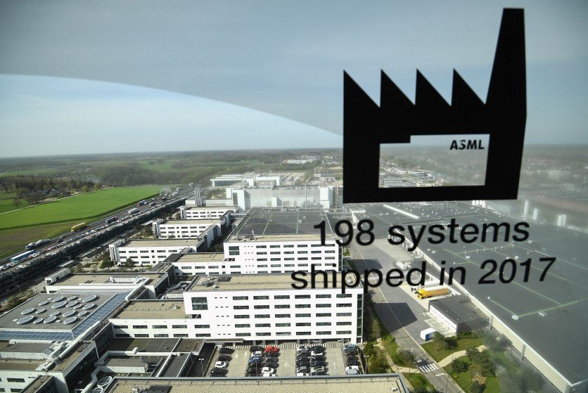
A view of ASML production plant, a Dutch company which is currently the largest supplier in the world of semiconductor manufacturing machines via photolithography systems in Veldhoven on April 17, 2018. They call it "the shrink" -- it's the challenge of how to pack more information onto the microchips which power everything from our phones to our computers, even our coffee machines. And pushing today's boundaries of science and technology is the Dutch company ASML, which since its foundation in 1984 has quietly become a world leader in the semiconductor business. (Photo by EMMANUEL DUNAND / AFP) EMMANUEL DUNAND/AFP via Getty Images
VELDHOVEN, Netherlands — ASML, the sole manufacturer of the extreme ultraviolet lithography machines that every cutting-edge chip on earth depends on, delivered a sweeping earnings beat Wednesday and issued its second upward guidance revision of 2026 — raising its full-year revenue forecast to between €43 billion and €45 billion and announcing plans to expand production capacity by 30% annually across both its EUV and deep ultraviolet product lines for each of the next two years.
The results, covering the second quarter ended June 28, drew an unambiguous line from the AI infrastructure arms race in American hyperscaler data centers to the factory floors of Veldhoven, a Dutch city most people cannot find on a map — and sent the company's shares up roughly 5% to 6% in early Amsterdam trading, according to ASML's Q2 2026 earnings results.
Read more: ASML Earnings Wednesday: EUV Bookings Will Show Whether the AI Chip Boom Is Sustainable
Quarter Beat Analyst Estimates Across All Metrics
ASML reported second-quarter net sales of €9.33 billion, surpassing analyst consensus estimates of approximately €8.80 billion. Net income reached €2.92 billion, ahead of the street's €2.62 billion estimate, while gross margin came in at 54.0% — above the company's own guidance of 51% to 52%. The installed base business, which covers service contracts, software upgrades, and field options for machines already deployed in customer fabs, generated €2.8 billion in revenue, roughly €300 million above management's projections.
ASML sold 86 new lithography systems in the quarter, up from 67 in the first quarter — a sequential jump that reflected how aggressively the world's largest chipmakers are adding capacity, per ASML's Q2 2026 SEC filing.
Guidance Raised to €43 Billion–€45 Billion
Two revisions and six months into 2026, ASML's full-year revenue floor has risen €9 billion from its original January guidance. The company entered the year expecting €34 billion to €39 billion in net sales; after its first-quarter results in April, it lifted that range to €36 billion to €40 billion. Wednesday's revision takes the full-year outlook to €43 billion to €45 billion — roughly $49 billion to $51 billion — with a gross margin of 54% to 56%, per ASML's Q2 2026 financial results.
For the third quarter alone, ASML guided net sales of €11.0 billion to €12.0 billion with a gross margin of 55% to 57%, implying a significant second-half revenue acceleration as system deliveries ramp.
"We expect third-quarter 2026 total net sales between €11.0 billion and €12.0 billion," said CEO Christophe Fouquet in ASML's earnings release. "Given the business dynamics discussed above, we now expect total net sales for 2026 to be between €43 billion and €45 billion."
AI Infrastructure Is the Engine
Fouquet was direct about what is driving the results. Artificial intelligence infrastructure investment, he said, is sustaining demand for advanced logic and memory chips from ASML's direct foundry customers — TSMC, Samsung, and Intel Foundry — and those customers are in turn accelerating their own capacity expansion timelines.
"Ongoing AI-related investments and continued progress in AI technologies are driving demand for advanced Logic and Memory chips, further strengthening the semiconductor industry's growth outlook," Fouquet said in ASML's earnings statement, noting that customer commitments now span ASML's full product portfolio and provide the company with "increased visibility into longer-term demand."
The demand signal reaching ASML travels a well-documented path. When Microsoft, Google, Amazon, or Meta commits capital to new AI training and inference infrastructure, those decisions translate into GPU and accelerator orders from Nvidia and AMD — which in turn require TSMC, Samsung, and Intel Foundry to add wafer capacity. That foundry expansion requires ordering lithography equipment from ASML, typically 12 to 18 months in advance. When ASML raises guidance and commits to a multi-year capacity expansion, it is surfacing demand signals that were set in motion at the hyperscaler level roughly two years prior.
Memory demand has been particularly acute. High-bandwidth memory chips — the stacked DRAM packages that feed data to AI accelerators at the speeds modern training workloads require — account for a major share of the memory revenue growth ASML is capturing, with demand expected to be significantly higher in 2026 than 2025.
How High-NA EUV Works, and Why Intel Went First
Alongside its financial results, ASML confirmed a technology milestone that signals where the entire industry is heading: Intel Foundry has become the first company to ship a high-volume logic product manufactured using High-NA EUV lithography — specifically, selected layers of chips in Intel's Core Ultra Series 3 "Panther Lake" family, produced on Intel's 18A process node at its facility in Hillsboro, Oregon, per ASML's High-NA EUV milestone announcement.
To understand the significance of that milestone, it helps to understand what High-NA EUV is and what it costs.
Standard EUV lithography uses 13.5-nanometer light generated by firing a high-powered carbon dioxide laser at droplets of molten tin, creating a plasma that emits in the extreme ultraviolet spectrum. That light is collected by a series of highly precise molybdenum-silicon multilayer mirrors — operating in vacuum, because all matter absorbs EUV radiation — and focused through an optical system onto a silicon wafer coated in photoresist. The light exposes a pattern defined by a reflective mask; the exposed photoresist is then chemically developed and the pattern etched into the chip layer. A single EUV machine, known as a scanner, weighs nearly 200 tons and costs approximately $180 million to $200 million per unit. At current specifications, standard EUV tools produce roughly 170 to 220 wafers per hour, as detailed in Tom's Hardware's technical breakdown.
High-NA EUV — formally ASML's Twinscan EXE:5200B — raises the numerical aperture of the optical system from 0.33 to 0.55. The numerical aperture governs how much light the projection optics can collect and how finely it can focus that light; a higher aperture enables smaller, more densely packed circuit features. At 0.55 NA, High-NA EUV can resolve features needed for chip nodes below 2 nanometers — geometries that the 0.33 NA system can only achieve through complex multi-patterning sequences that require multiple exposures and multiple masks, as Tom's Hardware explains in detail.
The engineering tradeoffs are real. To achieve 0.55 NA, ASML's engineers used an anamorphic optical design that applies 4x demagnification horizontally and 8x vertically — different reduction ratios in two directions, which requires the chip design and mask writing to account for asymmetric scaling. The field size shrinks from 26 millimeters by 33 millimeters on a standard EUV scanner to 26 millimeters by 16.5 millimeters on the EXE:5200B. A smaller field means more exposures per wafer, higher throughput requirements, and more expensive per-layer patterning costs. Each High-NA EUV exposure currently costs roughly 2.5 times more than a standard EUV exposure, and the machine itself carries a price tag of approximately $380 million to $400 million — roughly double a standard EUV tool, per ASML's official High-NA specifications.
Intel's deployment strategy reflects those economics precisely. The Panther Lake layers running on High-NA EUV are dual-qualified — the same layers can also be patterned on Intel's existing standard EUV fleet, with yields confirmed as matched across both platforms. That gives Intel production flexibility and lets the company gather real-world process data — uptime behavior, overlay accuracy, defect rates under production conditions — in advance of committing High-NA EUV to future nodes where it will carry greater wafer-level responsibility, per ASML's official milestone announcement.
"This milestone reflects the close technical collaboration between Intel and ASML and shows how High NA EUV can be integrated into advanced semiconductor manufacturing at scale," said Naga Chandrasekaran, Executive Vice President and General Manager of Intel Foundry, in ASML's announcement.
TSMC, by contrast, has stated it will skip High-NA EUV for its initial A14 (1.4nm effective) process node, opting instead to extend standard EUV tools through advanced multi-patterning. At TSMC's production scale — which runs orders of magnitude more wafers than Intel Foundry — the 2.5x cost premium per High-NA exposure does not yet deliver sufficient yield or density advantage to justify adoption over a multi-patterning approach using cheaper standard tools. Industry analysts and foundry observers expect TSMC to begin High-NA adoption around 2029 for its A14P or A10 generation, per industry analysts' assessment. Samsung has secured its own EXE:5200B systems and is targeting a comparable ramp timeline to Intel.
ASML plans to ship approximately ten High-NA systems in 2026, with per-unit revenue roughly doubling standard EUV pricing — meaning the High-NA mix will expand ASML's average selling price and sustain gross margin expansion even as unit volumes for standard EUV grow.
The 30% Capacity Commitment: What It Actually Means
The most consequential announcement Wednesday was ASML's plan to expand EUV and DUV production capacity by 30% annually in each of the next two years. In specific terms: ASML's 2026 capacity for its NXE (standard EUV) product line is approximately 65 systems. The company plans to add 30% for 2027 — bringing that to approximately 85 systems — and is investigating a further 30% increase for 2028. Its NXT (DUV immersion) line stands at approximately 130 systems in 2026, with the same 30% ramp planned for 2027 and another 30% under investigation for 2028, per ASML's Q2 2026 results announcement.
The lead time required to build lithography tools — among the most complex machines ever manufactured, with components sourced from suppliers across hundreds of companies and requiring precision optics polished to sub-nanometer tolerances — means this kind of commitment signals genuine multi-year demand conviction, not a near-term inventory build. ASML cannot ramp capacity on short notice; these are capital and supply chain decisions that take two or more years to execute.
Analysts took notice. "The message from bears has been that they are capacity-limited or that they don't grow," JPMorgan wrote in a note Wednesday. "The company is virtually guiding 30% growth in the next two years."
Javier Correonero, a senior equity analyst at Morningstar, told CNBC's post-earnings analysis that ASML was doing a great job bringing capacity in. Michael Roeg of Degroof Petercam offered a more pointed take on the same results: "Blowout results across the board. I wonder where they found this much new capacity."
Read more: ASML Raises Full-Year Guidance as Intel Ships First High-NA EUV Logic Chip
Does China's EUV Race Change the Calculus?
China's semiconductor ambitions add a layer of complexity that Wednesday's blowout numbers cannot fully paper over. CFO Roger Dassen confirmed that Chinese customers are expected to account for approximately 20% of 2026 net sales — down from roughly 33% in 2025. U.S.-led export restrictions already bar ASML from selling EUV tools and most advanced DUV machines to China.
The proposed Multilateral Alignment of Technology Controls on Hardware Act — the MATCH Act — would extend those restrictions further, banning even the DUV immersion systems that Chinese chipmakers currently source from ASML, and would also prohibit ASML from servicing machines already installed in Chinese fabs. Introduced in Congress on April 2, 2026, and passed out of the House Foreign Affairs Committee on April 22, the MATCH Act is not yet law. It has been reportedly softened from its original version but still includes a nationwide restriction on DUV immersion sales to China. It also contains a 150-day window for allied governments — principally the Netherlands and Japan — to implement equivalent controls or face unilateral U.S. enforcement, per the MATCH Act's legislative progress.
Chipmaking equipment is not a product that, once sold, requires no further attention. The machines need constant calibration, spare parts, software updates, and field engineering support. A servicing ban would effectively start a countdown on the usable life of China's existing installed base — a dynamic that analysts say may matter more to Chinese chipmakers in the medium term than the prohibition on new sales, as detailed in the MATCH Act's proposed servicing restrictions.
In absolute revenue terms, China's contribution to ASML continues to grow alongside overall sales growth even as its percentage share falls. But the trajectory is politically constrained, and any further legislative escalation poses a meaningful downside risk — particularly to ASML's high-margin service revenue.
What the capacity commitment announced Wednesday adds to that picture is geopolitically significant: Reuters reported in December 2025 that China had secretly completed a prototype EUV machine in Shenzhen, with working chip production expected between 2028 and 2030, as covered in Reuters' December 2025 reporting. A 30% annual EUV capacity ramp by ASML — compounding for two years — means that by the time any Chinese EUV alternative reaches commercial production, ASML's installed base, service ecosystem, and customer lock-in will be substantially larger than they are today. The capacity commitment is not just an earnings signal; it is, structurally, a multi-year competitive moat built in capital commitments rather than export controls.
That ASML is raising guidance and committing to a 60%+ capacity expansion despite a structural headwind from its largest 2025 market is itself a statement about the scale of AI-driven demand from non-Chinese customers.
What ASML Shares and the AI Chip Timeline Tell Investors
ASML shares have gained approximately 66% year to date, reflecting a market consensus that the company occupies a structurally irreplaceable position in global technology supply chains. There is no credible second source for EUV systems at commercial scale. No company other than ASML currently manufactures the machines that build the machines that build AI chips.
For investors and enterprise technology planners, Wednesday's results and the accompanying capacity commitment carry a clear message. The AI chip investment super-cycle — the multi-year wave of capacity spending flowing from hyperscaler AI ambitions down through foundries and ultimately into orders for ASML's tools — showed no sign of decelerating through the second quarter of 2026. The 30% capacity ramp plan, once it translates into full tool deliveries across 2027 and 2028, implies that the supply of cutting-edge chipmaking equipment will remain tight through at least the end of the decade, sustaining pricing power for ASML and urgency for every foundry in the queue.
ASML will update its longer-term financial outlook at its next Capital Markets Day, scheduled for June 10, 2027.
Frequently Asked Questions
Why can't any company other than ASML build EUV machines?
EUV lithography requires one of the most complex engineering systems ever built at commercial scale — a machine that fires a carbon dioxide laser at molten tin droplets 50,000 times per second to generate 13.5-nanometer light, then collects and focuses that light using mirrors polished to sub-nanometer tolerances in a hydrogen-buffered vacuum environment. The underlying intellectual property, developed through a public-private consortium funded by U.S. national laboratories in the 1990s, was consolidated when ASML acquired Silicon Valley Group in 2001 and partnered with German optics manufacturer Zeiss on the precision mirror systems. Canon and Nikon, the prior industry leaders, were denied access to that IP licensing. China completed a prototype EUV machine in Shenzhen in late 2025, but observers expect working chip production from that system between 2028 and 2030 — years behind ASML's production roadmap, per the technology's development history.
What is the difference between High-NA EUV and standard EUV, and why does it matter?
Standard EUV tools use a numerical aperture (NA) of 0.33, which determines how finely the optical system can focus light onto a wafer. High-NA EUV raises that to 0.55 — a 66% increase — enabling the smaller, denser circuit features required for chip designs at and below the 2-nanometer threshold. The tradeoff is cost: each High-NA EUV exposure currently costs roughly 2.5 times more than a standard EUV exposure, and the machine itself costs approximately $380 million to $400 million versus $180 million to $200 million for a standard EUV tool. That cost gap is why TSMC has opted to skip High-NA for its initial A14 node and use multi-patterning with cheaper standard EUV instead — and why Intel's Panther Lake deployment qualifies High-NA for specific layers only, rather than replacing the entire lithography flow, as explained in our full explainer on High-NA EUV.
What would the MATCH Act mean for ASML and AI chip supply if it becomes law?
If enacted, the MATCH Act would ban ASML from selling its remaining accessible products to Chinese chipmakers — principally the DUV immersion lithography machines that companies such as SMIC and Hua Hong currently use to manufacture less-advanced semiconductors. More significantly, the bill would also prohibit ASML from servicing machines already installed in Chinese fabs. Because chipmaking equipment requires continuous calibration, software updates, and physical maintenance to maintain process stability, a servicing ban would gradually degrade the performance and yield of China's existing installed base without any new export. The bill, as of July 2026, has passed committee in the House but is not yet law; it also contains a 150-day window for allied governments — the Netherlands and Japan — to implement equivalent controls before the U.S. would act unilaterally. ASML has declined to comment on the proposed legislation, per the MATCH Act's full text.
How should AI infrastructure investors and enterprise planners read ASML's capacity commitment?
ASML's 30% annual ramp plan for 2027 — and its investigation of a further 30% for 2028 — is a leading indicator of where the semiconductor supply chain will be in two to three years. Because ASML tools require 12 to 18 months of manufacturing lead time and customers must commit to orders well in advance, the capacity expansion reflects foundry demand that is already committed, not speculative. For investors, it signals that the AI chip super-cycle is in early-to-mid innings: the equipment to sustain the next phase of GPU and accelerator production is being ordered and built today. For enterprise planners, it implies that supply of cutting-edge chipmaking equipment will remain constrained — and therefore compute will remain expensive at the frontier — well into 2028, as detailed in ASML's Q2 2026 results and outlook.

-
 C114 Communication Network
 -
 Communication Home
