
 Search

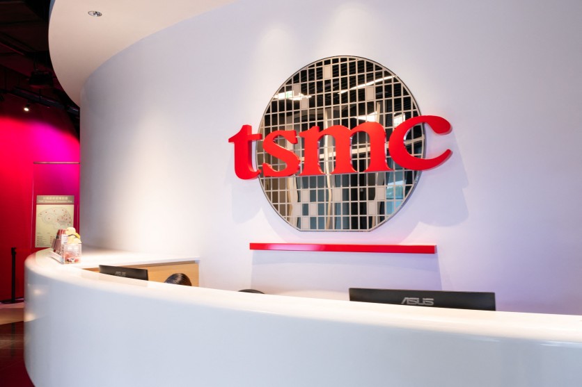
The TSMC logo is displayed at the Taiwan Semiconductor Manufacturing Company branch and Innovation Museum, highlighting the company branding and signage inside and outside the site in Hsinchu, Taiwan, January 27, 2026. As the worlds leading semiconductor foundry, TSMC plays a central role in the global chip supply chain that powers computers, smartphones, servers and many modern industries. Jimmy Beunardeau/Hans Lucas / AFP via Getty Images
Taiwan's silicon foundry sector posted aggregate revenue of US$15.13 billion in June 2026 — up 54.0% from a year earlier and 5.9% from May — according to DigiTimes analysis published Monday. The headline number tells one story. The more significant signal is the one buried in the sub-sector data: every single one of the 13 segments DigiTimes tracks across Taiwan's semiconductor value chain posted positive year-over-year growth for the month. Not 12 of 13. Not most. All of them.
That full-sector sweep has not happened in prior technology-driven booms, and the reason it is happening now is structural rather than coincidental. AI accelerator chips — the Nvidia GPUs, AMD Instinct cards, and custom ASICs that hyperscale cloud providers are deploying by the millions — require something prior consumer technology platforms did not: simultaneous, irreducible demand on multiple distinct layers of the supply chain at once. A PC or smartphone boom strains silicon fabrication. An AI infrastructure buildout strains silicon fabrication and advanced packaging and high-bandwidth memory and the substrate materials that interconnect all of them. Remove the shortage at any one layer and the shortage at the adjacent layer remains. That is why the DRAM sector nearly quadrupled year-over-year in June while the packaging houses and substrate makers expanded in lockstep with the foundries.
TSMC's own June numbers anchored the data: the company reported consolidated revenue of NT$442.68 billion (approximately US$13.8 billion) for the month, as confirmed in TSMC's Form 6-K filing with the U.S. Securities and Exchange Commission, an increase of 6.2% from May and 67.9% from June 2025. For the first six months of 2026, TSMC's cumulative revenue reached NT$2.404 trillion (approximately US$75 billion), up 35.6% from the same period a year earlier. The company is scheduled to report full second-quarter 2026 results on Thursday, July 16, in a conference call beginning at 2:00 AM ET, where investors will watch for any revision to management's full-year growth outlook, updates on advanced packaging capacity, and pricing commentary for its most advanced process nodes.
Read more: TSMC Sets All-Time Revenue Record: AI Demand Has Rewritten Its Calendar
June Reversed a Four-Year Seasonal Pattern at TSMC
TSMC recorded a 6.2% month-over-month revenue increase in June — an unusual result for a month that had seen sequential declines in each of the prior four years. In June 2025, for instance, TSMC's revenue fell 17.7% from May before recovering sharply in the second half of the year. That seasonal dip has been a reliable feature of TSMC's revenue calendar because June historically sits between the spring ramp-up of consumer device launches and the back-half demand surge. This June, that pattern broke.
The reason, according to Sravan Kundojjala of SemiAnalysis, is that AI chip supply remains structurally constrained: TSMC's cutting-edge 3-nanometer process capacity is fully booked by AI GPU and server CPU customers through year-end. When your most expensive capacity is sold out through the calendar, seasonal softness in consumer demand no longer dents your sequential revenue line — because the customers filling your fabs are not selling smartphones, they are building AI infrastructure that runs 24 hours a day regardless of consumer purchase cycles.
TSMC commands approximately 73% of the global pure-play foundry market as of the first quarter of 2026, according to Counterpoint Research. Its customer base spans virtually every major semiconductor designer that matters to AI: Nvidia and AMD for compute accelerators, Apple for its M-series and A-series processors, Qualcomm for wireless chips, and the in-house silicon teams at Amazon, Google, and Microsoft building custom AI accelerators for their own cloud workloads.
Analysts project TSMC will report approximately $40 billion in second-quarter 2026 revenue — up from $30.07 billion in the same quarter a year earlier — with earnings per ADR of roughly $3.81, up from $2.47 in Q2 2025. Wall Street's consensus ahead of Thursday's report put revenue at approximately $40.02 billion. The company's own guidance, issued in April, called for $39.0 billion to $40.2 billion in quarterly revenue. Citi analyst Laura Chen has already raised her price target for TSMC's Taiwan-listed shares to NT$3,800 from NT$2,875, citing expectations that management will revise its full-year growth outlook above 30% in dollar terms and raise wafer prices for its 2nm and 3nm processes.
Memory Nearly Quadrupled — and That Signal Points Beyond One Sector
The memory sub-sector's near-quadrupling of year-over-year revenue in June is not primarily a Taiwan story — the dominant memory manufacturers (SK Hynix and Samsung for DRAM; Kioxia and Micron for NAND) are not Taiwanese. What the Taiwan data captures is the packaging, testing, and substrate work that flows through Taiwanese companies on behalf of those memory manufacturers. When memory revenue in the Taiwan supply chain nearly quadruples, it reflects the surge in high-bandwidth memory (HBM) packaging demand that is flowing through OSAT companies like ASE Technology and through substrate makers whose ABF and BT substrate products are essential to HBM assembly.
The mechanism is worth understanding. Each AI GPU currently requires HBM stacks — clusters of DRAM dies assembled in 8- or 12-layer configurations. A 12-layer HBM stack uses twelve individual DRAM dies where a standard server memory module uses none. As hyperscalers have deployed millions of AI accelerators over the past year, the incremental DRAM demand created by those HBM requirements has absorbed capacity at a time when memory suppliers had already constrained new production following the 2022 industry downturn. Memory manufacturers emerged from that downturn with a stronger commitment to capital discipline — limiting capacity additions rather than racing to oversupply — and the AI demand surge hit a market that was structurally unwilling to add supply aggressively. The result: a memory cycle that analysts believe will remain in a supply-demand imbalance through at least 2027.
UMC, the second-largest Taiwanese pure-play foundry, reported a 22.9% year-over-year revenue increase for June, with first-half cumulative revenue reaching NT$129.8 billion, up 11.3% from the same period last year, according to UMC's June filing. In its first quarter, UMC's 22-nanometer logic revenue hit a record high, driven by demand for display driver ICs, networking chips, and power management circuits — specialty-node products that run on mature process technology rather than cutting-edge nodes, suggesting the upcycle extends well beyond the leading-edge race.
CoWoS, ABF Substrates, and Why This Boom Has No Single Choke Point
Understanding why this upcycle is propagating through all 13 sub-sectors simultaneously requires understanding what happens between the wafer coming out of a TSMC fab and an AI accelerator landing in a data center rack. The answer is: quite a lot, and none of it is simple.
CoWoS — why packaging became the bottleneck: After TSMC fabricates a logic die at the 3-nanometer node, that die cannot be used as an AI accelerator without being integrated with high-bandwidth memory stacks in a complex 2.5D packaging process. TSMC's proprietary technology for this integration is called CoWoS (Chip-on-Wafer-on-Substrate). The process places the logic die and HBM stacks on a silicon interposer — a thin slab of silicon that acts as a microscopic circuit board — which then allows data to flow between the logic and memory at speeds and bandwidths impossible with conventional 2D packaging. Nvidia's Blackwell-generation GPUs require memory bandwidth exceeding 9,000 gigabytes per second; achieving that throughput physically requires the logic and memory dies to be separated by microns rather than millimeters. Only CoWoS does that at production scale today.
TSMC is in the process of expanding CoWoS capacity from approximately 35,000 wafer starts per month in late 2024 to a targeted 120,000 to 140,000 wafer starts per month by the end of 2026 — a roughly fourfold increase, according to TrendForce's CoWoS capacity analysis. Nvidia has reportedly secured more than 60% of that capacity for its own chip programs. Even at four times the prior output, CoWoS capacity remains the primary constraint on how many AI accelerators can be delivered per quarter. Setting up a new packaging facility requires specialized equipment — ultra-precise pick-and-place machines, thermal compression bonders — that itself carries 12- to 18-month lead times, preventing rapid capacity addition regardless of capital availability.
ASE Technology, Taiwan's largest outsourced semiconductor assembly and test company, raised its guidance for advanced packaging revenue to more than US$3.5 billion for full-year 2026, up from $3.2 billion guided the prior quarter, according to its Q1 2026 earnings call, reflecting how the CoWoS demand surge is propagating into every company in the packaging tier.
ABF substrates — the material constraint beneath the packaging constraint: Under the CoWoS interposer sits an ABF (Ajinomoto Build-up Film) substrate, the organic circuit board that connects the entire assembled chip package to the server's printed circuit board. This material — manufactured by a single Japanese company, Ajinomoto, which controls more than 95% of the global ABF film market — is now in its own structural shortage. In May 2026, Ajinomoto announced a 30% price increase on ABF film, effective in the third quarter.
The price increase reflects real physical scarcity. AI chip packaging layers are evolving from 3+3 configurations (three routing layers above and below the core) to 11+11 and ultimately 13+13 — dramatically increasing the amount of ABF material consumed per chip. Each AI GPU requires one to two large ABF substrates measuring 70mm × 70mm or larger, roughly double the footprint of a consumer CPU substrate. Taiwan's major substrate makers — Unimicron, Nan Ya PCB, and Kinsus Interconnect Technology — are operating at full capacity, with advanced production lines heavily pre-allocated to AI clients. Lead times for ABF substrates have extended from a normal 12–16 weeks to 20–30 weeks.
Compounding the substrate shortage is an upstream materials constraint: Ajinomoto's ABF film production requires T-glass fiber cloth, which is itself in short supply. Approximately 70% of T-glass fiber cloth demand is currently allocated to ABF substrates, and that shortage is projected to persist through 2027, according to TrendForce's glass fiber analysis. Ajinomoto announced a ¥1.2 billion (~US$7.6 million) investment in a third ABF plant in Gifu Prefecture, with production targeted for 2032 — illustrating that the material-level supply constraint cannot be resolved this decade regardless of capital commitment.
The cascade is complete: AI chip demand tightens TSMC's advanced node capacity, which tightens CoWoS packaging capacity, which tightens ABF substrate demand, which tightens T-glass fiber cloth supply. Each layer has its own lead time and capital cycle, and none of them can be shortcut. This is the engineering reality that explains why Taiwan's entire semiconductor ecosystem grew in June rather than just its leading-edge foundry.
Read more: TSMC Q2 Earnings July 16: Three CoWoS Signals That Test AI's Spending Ceiling
What the Full-Sector Sweep Means — and What to Watch Thursday
The breadth of the June data distinguishes the current AI-driven expansion from every prior semiconductor boom that industry analysts track. The PC upcycle of the early 2020s ran hot in logic and DRAM while packaging houses and specialty-node foundries lagged. The 2017–2018 DRAM boom lifted memory players while logic foundries moved independently. The mobile boom of 2021 concentrated demand at TSMC and left OSAT companies scrambling for non-phone work. This time, the demand propagation is simultaneous across all five tiers of the value chain — logic silicon, memory, advanced packaging, OSAT, and substrates — because the end product consuming all of them is the same: an AI accelerator chip that physically requires all five at once.
For readers tracking AI infrastructure costs and timelines, the practical implication is that no single capacity addition at any one layer will resolve the AI chip supply constraint. TSMC can expand CoWoS capacity fourfold; Ajinomoto cannot add a third ABF plant until 2032. The system is supply-constrained at a layer below the layer most people are watching.
Thursday's TSMC earnings call will be the next major data point. Wall Street will listen for three signals: whether management raises its full-year revenue growth guidance above the existing 30%-plus target in US dollar terms; whether TSMC signals any acceleration in CoWoS advanced packaging capacity beyond the 120,000–140,000 wafers per month already planned; and whether the company provides pricing commentary on its 2-nanometer process node, which is expected to begin ramping in the second half of this year. Given the June revenue print and the all-sector sweep, the bar going in is already high — and the earnings call is likely to set the market's expectations for AI chip supply through at least 2027.
For consumers, the near-term consequence is more direct: as TSMC gains pricing power on its 3nm and 2nm nodes and substrate and packaging costs rise across the board, those increases have historically made their way into flagship smartphone and laptop prices within two to three quarters. If you are planning a major technology purchase for the holiday season, the June supply chain data represents one reason prices at the high end may be moving rather than falling.
Frequently Asked Questions
Why is this semiconductor upcycle different from past boom cycles?
Prior semiconductor booms concentrated in a single supply-chain layer: PC demand surged at logic foundries but left memory and packaging houses unaffected; memory booms in 2017–2018 lifted DRAM prices while specialty-node foundries operated normally. The current AI infrastructure cycle creates demand that is physically irreducible across multiple distinct layers simultaneously — advanced logic silicon for the GPU or ASIC die, CoWoS advanced packaging to integrate it with HBM memory stacks, the HBM memory itself, ABF substrates to mount the completed package on, and the T-glass fiber cloth that goes into those substrates. You cannot build an AI accelerator while shortcutting any of those layers. That multi-layer demand architecture is the engineering reason every tracked sub-sector in Taiwan grew at once in June 2026, and it is why industry analysts expect the supply-demand imbalance to persist well into 2027 across multiple tiers simultaneously.
What is CoWoS packaging, and why can't TSMC just build more of it quickly?
CoWoS (Chip-on-Wafer-on-Substrate) is TSMC's advanced packaging technology that places a logic die — the GPU or AI chip — and high-bandwidth memory stacks on a silicon interposer, enabling data to flow between them at speeds and densities impossible with conventional 2D packaging. Every Nvidia H100, H200, and Blackwell GPU requires CoWoS; so do most competing AI accelerators. TSMC is expanding CoWoS capacity from roughly 35,000 wafer starts per month in late 2024 to an estimated 120,000 to 140,000 by year-end 2026 — a fourfold increase that still leaves CoWoS as the primary bottleneck for AI chip delivery. The reason capacity cannot be added faster is that CoWoS facilities require specialized assembly equipment — thermal compression bonders, ultra-precise pick-and-place machines — that itself takes 12 to 18 months to manufacture and install. Capital alone cannot compress that timeline.
What does the ABF substrate shortage mean for AI chip delivery timelines?
ABF (Ajinomoto Build-up Film) substrates are the organic circuit boards that mount completed chip packages onto the server's main printed circuit board. Ajinomoto controls more than 95% of the global supply of ABF film — the critical dielectric material inside those substrates — and raised its prices 30% effective Q3 2026. Taiwan's major substrate makers (Unimicron, Nan Ya PCB, and Kinsus Interconnect Technology) are running at full capacity with AI chip programs pre-allocated through year-end, and lead times have extended from a normal 12–16 weeks to 20–30 weeks. Ajinomoto's investment in a third ABF production facility targets a completion date of 2032, which means this specific material constraint will not be resolved at the upstream level before the end of the decade. In practice, companies building AI infrastructure should factor ABF substrate lead times into procurement planning: substrate allocation, not wafer availability, may be the determinant of delivery timing for certain high-end AI chip configurations through at least 2027.
How might this supply chain data affect the price of smartphones and laptops?
TSMC's growing pricing power over its 3-nanometer and 2-nanometer nodes — the processes used to fabricate Apple's A-series and M-series chips, Qualcomm's flagship Snapdragon processors, and other premium mobile silicon — means that wafer cost increases are a real input to consumer device manufacturing economics. Historically, those upstream cost increases reach retail prices within two to three product cycles, which translates to roughly two to three quarters for flagship smartphones and laptops. Rising substrate and packaging costs compound the wafer-level pressure. Analysts at Citi have noted that the magnitude of any retail price movement depends on how much each device brand absorbs at the component level before passing costs through, but the directional pressure from the current supply chain data runs toward higher, not lower, prices for high-end consumer devices in the second half of 2026 and into 2027.

-
 C114 Communication Network
 -
 Communication Home
