Search


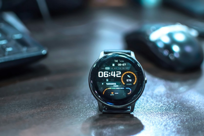
Al Amin Mir/Unsplash.com
The global display industry has spent years promising that microLED — a technology that offers brighter images, longer panel lifetimes, and dramatically lower power consumption than conventional OLED screens — would transform wearable devices. As of today, the MicroLED Industry Association (MIA), a standards and advocacy body representing more than 55 manufacturers, chipmakers, and equipment suppliers, is now willing to put a date on that transformation: the end of 2027.
The MIA's new whitepaper, published this morning and focused specifically on wearable display applications, describes end-2027 as a "credible target" for the first commercial mass-production runs of microLED smartwatch panels — provided that four production players currently in various stages of development each hit their own internal milestones, and that a critical engineering challenge in backplane transistor architecture is resolved alongside the better-known mass transfer bottleneck.
For consumers, the practical question is straightforward: should you buy a current-generation smartwatch — today's flagship being Samsung's Galaxy Watch Ultra 2, which shipped in August with a 1.52-inch (38.6 mm) Super AMOLED display reaching 5,000 nits at $699.99 — or hold on another fourteen months and see whether your next device has a fundamentally different kind of screen? The answer, the MIA says, depends on what "credible" means in engineering terms.
What MicroLED Actually Is — And Why OLED Users Should Care
A microLED display is exactly what the name implies: an array of microscopic light-emitting diodes, each one measuring between 3 and 20 micrometers (0.003 to 0.020 mm, or roughly one-fifth the width of a human hair), arranged in a grid where each pixel is its own self-emitting semiconductor device. Unlike OLED, which generates light through organic carbon-chain compounds, microLED uses inorganic gallium nitride (GaN) crystals — the same material class as the high-efficiency LEDs in modern lighting.
That material difference translates to three practical advantages for smartwatch users. MicroLED can reach peak brightness levels exceeding 10,000 nits — well above the 5,000-nit ceiling of today's best AMOLED displays — while consuming less power per nit delivered. For outdoor legibility, that matters. For battery life, it matters even more. MicroLED panels are also resistant to the burn-in failure mode that affects OLED screens displaying static images for extended periods — a particularly relevant attribute for smartwatch always-on displays that show the same interface elements for years. And the underlying semiconductor physics of gallium nitride LEDs means a microLED panel should outlast its OLED counterpart by a substantial margin, relevant for users who carry years of health data they prefer not to migrate.
One commercial microLED smartwatch has already cleared the manufacturing hurdle. The Garmin Fenix 8 Pro MicroLED, released in September 2025 at $1,999.99 for the 51mm model, features a 1.4-inch, 4,500-nit display panel produced by AU Optronics — the first consumer wearable to bring this technology to market. The challenge that remains is not whether microLED works at the device level, but whether it can reach cost-competitive mass production volumes accessible to mainstream consumers. That is the question the MIA's end-2027 target is designed to answer.
The Manufacturing Bottleneck No One Has Fully Solved
Building a microLED smartwatch display requires placing millions of individually tested semiconductor dies — each smaller than a dust particle — with micrometer-level accuracy onto a glass or flexible backplane substrate, then electrically connecting every one of them. The process is called mass transfer, and it is the central reason microLED has been perpetually several years away from widespread consumer availability.
The yield requirement for commercial viability is unforgiving. Display manufacturing engineers measure yield in "nines" — the number of nines after the decimal in a percentage. At 99% yield (two nines), a wearable display with 500,000 pixels would have roughly 5,000 defective emitters: visually catastrophic, economically unacceptable. Five-sigma yield — 99.999%, or five nines — is the industry consensus threshold for cost-competitive mass production. Current conventional pick-and-place transfer methods typically achieve 95–98% yield, which is why microLED products have so far been limited to large-format commercial displays where individual pixel repair is economically feasible and panels do not need to be produced in millions of units per month.
Smartwatch panels change that equation. A 1.5-inch display needs roughly a tenth of the chip count of a smartphone screen, which is why the industry has consistently identified wearables as the first viable mass-market application. The MIA's end-2027 target is based on this logic: smaller panels mean fewer transfer operations per unit, which means five-sigma yield is achievable at wearable scales even with current-generation transfer equipment — but only if the four manufacturers named in the whitepaper actually deliver on their current production roadmaps.
The Four Players — Where Each One Stands Today
Samsung Display: The Pilot Line at Asan
Samsung Display, the world's largest OLED panel manufacturer and the dominant supplier for its parent company's Galaxy Watch lineup, began construction of a 5.5-generation pilot production line at Asan in South Korea in June 2026. The pilot is intended to validate manufacturing parameters, not to produce commercial volumes — but the company has indicated it will make a mass production investment decision in the second half of 2027 based on the pilot's yield and cost data.
Notably, Samsung Display's current microLED chip supplier for the Asan prototype is Chinese LED supplier Sanan Optoelectronics — not a Taiwanese supplier. This supply-chain configuration is worth tracking for anyone following Samsung's microLED transition, as supplier diversification and geopolitical considerations could affect production timelines independent of the core manufacturing engineering.
If the pilot succeeds and Samsung commits to mass production in the second half of 2027, the company would be positioned to supply its own Galaxy Watch series with microLED panels in the 2028 generation — consistent with the MIA's end-2027 credible-target framing.
AUO: The Most Commercially Operational Line
Display panel maker AUO (AU Optronics), Taiwan's second-largest display company, has the most commercially operational microLED transfer infrastructure among the four players named by the MIA. Its existing mass transfer line, located at AUO's Longtan production facility in the Hwa Ya Technology Park in Taoyuan, has been used for limited commercial microLED production runs — including the display panel in the Garmin Fenix 8 Pro MicroLED. A new Gen 4.5 line, designed for the higher throughput and tighter pitch tolerances required for wearable displays at mass-production volumes, is targeted for first production in the first half of 2027.
AUO's microLED chip supply comes primarily through its partnership with PlayNitride, cemented by an approximately $21.3 million USD investment in the Taiwanese microLED specialist.
One supply-chain development worth monitoring: AUO's L3D fabrication facility — its primary production line for Garmin's current-generation smartwatch OLED panels — is reportedly scheduled to close in the first half of 2027, according to a TrendForce industry analysis. The closure is part of AUO's broader consolidation into next-generation display architectures, but it creates a transition gap in its established wearable display business that coincides precisely with the ramp-up period for the Gen 4.5 microLED line.
PlayNitride: The Vertically Integrated Specialist
Taiwan-based microLED maker PlayNitride, based in Miaoli County, occupies a unique position in the microLED supply chain: it is the only major player that controls the entire production process from epitaxial wafer growth through finished chip manufacturing to mass transfer. This vertical integration gives PlayNitride finer control over the yield parameters at each stage of production — a potential advantage as the industry pushes toward five-sigma transfer yields.
The company's current production capacity targets 10,000 wafers per month, and it has committed to shipping to customer production lines by the end of 2027. Its relationship with AUO provides both capital and a confirmed downstream customer for wearable display applications.
VueReal: The Architectural Bet
Canadian microLED company VueReal, headquartered in Waterloo, Ontario, is pursuing the most architecturally differentiated approach among the four MIA-cited players. Its EcoVue platform — announced at CES 2026 in January and demonstrated in a solar-integrated variant at SID Display Week 2026 in May — uses a process the company calls MicroSolid Printing: microLED emitter material is loaded into cartridge containers and deposited onto the backplane substrate in a parallel printing operation, rather than being individually picked and placed as separate die.
The practical significance of this distinction is yield. Conventional mass transfer approaches pick up and place individual microLED chips; every placement is a discrete operation that can fail. VueReal's cartridge printing deposits arrays of emitters simultaneously, which the company argues structurally avoids the per-die yield accumulation problem. The tradeoff is that the cartridge printing process is newer and has less production history than established transfer methods — meaning its real-world five-sigma yield remains to be demonstrated at commercial scale.
VueReal has stated its goal of achieving cost parity with premium OLED displays within approximately two years, implying a target of around 2028 — slightly beyond the MIA's end-2027 target but consistent with the broader industry timeline.
The Engineering Condition the Whitepaper Emphasizes: Beyond Mass Transfer
The MIA whitepaper's credible-target framing is conditional, and understanding those conditions requires looking past the mass transfer headline at a less-discussed bottleneck: backplane transistor architecture.
Every self-emissive display — OLED or microLED — requires a transistor backplane that tells each pixel when to emit light and at what intensity. For OLED, this control is achieved through a relatively efficient current-control architecture where each pixel's organic emitter responds smoothly to analog current levels. MicroLED requires a different approach. Because inorganic LEDs respond nonlinearly to current at the low intensities needed for typical wearable display brightness levels, the industry has converged on pulse-width modulation (PWM) driving: each microLED is switched on and off thousands of times per second, with the ratio of on-time to off-time controlling perceived brightness. PWM driving requires a substantially more complex transistor circuit per pixel than OLED's current-control approach — more transistors per pixel means more silicon area per pixel, which translates to higher power consumption from the backplane electronics, partially offsetting microLED's efficiency advantage over the emitters themselves.
A second backplane consideration runs alongside PWM efficiency: LTPO compatibility. The LTPO variable-refresh-rate display technology (Low-Temperature Polycrystalline Oxide) pioneered for wearables by Apple in the Apple Watch Series 5 enables displays to drop their refresh rate to as low as 1 Hz for static always-on content — the key mechanism behind modern smartwatches' always-on display efficiency. Current prototype microLED panels use conventional backplanes, not LTPO-equivalent architectures. Combining LTPO's variable-refresh-rate capability with microLED's PWM driving circuit requirements is an active area of development that has not yet been demonstrated at mass-production scale. Until it is, end-2027 microLED smartwatches will likely lack the always-on display power efficiency that LTPO-based AMOLED devices have offered since 2019 — a meaningful caveat for buyers who rely on always-on watch faces.
What the Current AMOLED Benchmark Means for the Timeline
The Samsung Galaxy Watch Ultra 2, which launched in August 2026 as the brightest consumer smartwatch display ever shipped, provides a useful benchmark for understanding how much ground microLED needs to cover before early adopters will notice the difference.
The Watch Ultra 2's 5,000-nit Super AMOLED panel is — by any practical outdoor-legibility standard — excellent. To be a compelling upgrade over that display, a first-generation microLED wearable would need to offer meaningfully better battery life, visibly superior brightness in direct sunlight, or both. The engineering conditions described above — mass transfer yield, PWM backplane efficiency, and LTPO compatibility — are precisely the factors that determine whether end-2027 microLED panels clear that bar or merely match it at higher manufacturing cost.
The MIA's whitepaper positions end-2027 as "credible" rather than "confirmed" for exactly this reason: the four production players are on track, the engineering problems are defined, and the solutions are in active development — but the gap between a successful pilot and cost-competitive mass production remains real, even as it has closed faster than expected in this technology cycle.
Realistic Expectations for Consumers
Based on the MIA whitepaper's findings and the production roadmaps of the four named players, here is what a technically informed consumer should expect.
End-2027 is a production milestone, not a retail launch date. When manufacturers announce mass production capability, the first commercial volumes go to device manufacturers who have been in engineering qualification for 12–18 months. The first retail microLED smartwatches at competitive prices will likely appear in 2028 models, assuming end-2027 production targets are met.
First-generation microLED wearables will carry a premium. Even at the five-sigma yields the industry is targeting, microLED manufacturing remains more capital-intensive than AMOLED. Early devices are likely to appear in flagship-tier products at flagship-tier prices before costs moderate.
The brightness advantage will be immediately visible. The battery advantage may not be. Until LTPO-compatible microLED backplanes reach production, the power consumption advantage over state-of-the-art AMOLED+LTPO devices will be smaller than the technology's theoretical potential. MicroLED's most defensible near-term advantage is brightness and burn-in elimination, not necessarily battery life extension.
The 2028–2029 generation is the more probable inflection point. If end-2027 mass production targets are met on schedule, the 2029 wearable generation is likely to be the first year in which microLED devices from multiple manufacturers compete at scale — when yields have matured, costs have begun to fall, and LTPO-compatible backplane designs have entered production.
About the MicroLED Industry Association
The MicroLED Industry Association, founded to accelerate the commercialization of microLED technology through shared standards and cross-industry coordination, now represents more than 55 companies spanning the full supply chain from LED epitaxy through mass transfer equipment to end-device manufacturing. Its whitepapers represent consensus positions across its membership and are used by device makers and investors as reference timelines for technology planning.
Today's wearable display whitepaper is the association's most specific public commitment to a production timeline for the consumer market's highest-volume microLED application category.
Exchange rate as of November 9, 2026; conversions are approximate.
Frequently Asked Questions
When will microLED smartwatches be available to buy?
One commercial microLED smartwatch is already available: the Garmin Fenix 8 Pro MicroLED, released in September 2025 at $1,999.99 for the 51mm model, delivering 4,500 nits from an AU Optronics-produced display. The MicroLED Industry Association's end-2027 target refers to mass-production capability by multiple manufacturers, which would likely yield the first broadly available, competitively priced retail devices in 2028 smartwatch generations.
How does a microLED display differ from OLED?
MicroLED uses inorganic gallium nitride (GaN) semiconductor emitters, while OLED uses organic carbon-chain compounds. The key practical differences for smartwatch users are: microLED can reach significantly higher peak brightness (above 10,000 nits versus roughly 5,000 nits for the best AMOLED panels), it does not suffer from burn-in caused by static images, and its inorganic emitters have longer operational lifetimes. The tradeoff is manufacturing complexity — placing millions of microscopic LED chips with the precision needed for commercial yields remains the central challenge.
Will Apple Watch get a microLED display?
Apple has not confirmed microLED plans for the Apple Watch. TrendForce has noted that Apple has not entirely abandoned the microLED smartwatch market and may revive related plans through a renewed supply-chain strategy, but no specific timeline or product announcement has been made as of the date of this article.
What is mass transfer, and why does it matter for microLED manufacturing?
Mass transfer is the process of placing millions of individually tested microLED semiconductor chips — each just a few micrometers across — onto a backplane substrate with micrometer-level accuracy. It is the central bottleneck for microLED at consumer scale because the yield requirement is extremely demanding: the industry targets 99.999% transfer yields for cost-competitive wearable production, while conventional transfer methods currently achieve 95–98%.
What is the MicroLED Industry Association?
The MicroLED Industry Association is a standards and advocacy body representing more than 55 companies across the microLED supply chain, from LED chip manufacturers and mass transfer equipment suppliers to panel makers and device manufacturers. It publishes whitepapers and develops shared standards to accelerate microLED commercialization. Its wearable display whitepaper, released November 9, 2026, identifies the manufacturing milestones required for end-2027 mass production of microLED smartwatch displays.

-
 C114 Communication Network
-
 Communication Home