Search


Spilglobal.com
Nvidia is funding new production lines at Taiwanese chip-packaging company SPIL that cover bumping, interposer wafer fabrication, assembly and testing, according to the agreement Nvidia announced Tuesday. An interposer is the silicon routing layer that connects an AI processor to its memory stacks. Making interposers has typically been TSMC's CoWoS front-end step, so the scope points to Nvidia financing a second source for part of the front half of an AI chip package, not only more back-end floor space. Neither company has said how the interposers will be made or under what license.
Nvidia released the multiyear agreements at 5:18 p.m. ET Tuesday, naming six partners: Amkor, Foxconn, Kinsus, Samsung Electro-Mechanics, SPIL and TSMC. SPIL said Wednesday in Taiwan that it will triple its advanced packaging capacity there by mid-2029, and Nvidia described its funding as multibillion-dollar without giving a figure.
The timing matters for anyone planning around AI accelerator supply. Kinsus substrate production for Nvidia starts in the second half of 2027, Kinsus targets added capacity in the third quarter of 2028, and SPIL's tripling lands in mid-2029. No capacity from this agreement is on the calendar before 2027.
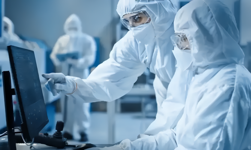
SPIL Lines Span Bumping, Interposer Wafer Fabrication, Assembly and Testing
Nvidia's release says the SPIL project includes new production lines with turnkey support across four steps. Bumping places solder bumps on a chip's contact pads so the die can be can be mounted face-down on its package. High-bandwidth memory uses very wide interfaces that need an interposer between processor and memory, and interposers cost far more to make than ordinary circuit boards.
Nvidia's operations chief, Debora Shoquist, said the agreement helps secure the packaging capacity and turnkey production Nvidia needs to meet demand, according to Taipei Times. SPIL chairman and president C.W. Tsai said it strengthens SPIL's ability to support next-generation packaging for AI systems. Reuters reported, citing an industry executive, on Nov. 6 that Nvidia was financing SPIL's expansion with billions of dollars.
SPIL is part of ASE Technology Holding, described as the world's biggest contract packager.
What Is CoWoS, and Why Does It Cap AI Accelerator Output?
CoWoS, short for chip-on-wafer-on-substrate, splits into two stages. In the first, chips are attached to a silicon interposer. In the second, that interposer is bonded to a package substrate. Contract packagers, including ASE, Amkor and SPIL, have handled the second stage under TSMC licenses, while outsourced volumes of the first stage were limited. TrendForce News, citing an ETNews report, said TSMC is expanding outsourcing of the first stage.
The squeeze is concentrated. TrendForce News, citing Mydrivers, said Nvidia reserved roughly 800,000 to 850,000 wafers of 2026 CoWoS capacity, and the report estimated a 2026 supply-demand gap near 20%. That is why a funded second pool of interposer and assembly lines draws attention beyond its own size.
Interposer Type, Licensing Terms and Baseline Capacity Remain Undisclosed
The announcements leave the key numbers out. SPIL gave no baseline for current capacity, so "triple" has no absolute value yet. Nvidia's release speaks of Nvidia-dedicated contracted capacity rising by mid-2029 without a multiple, while SPIL's statement describes its overall advanced packaging capacity in Taiwan, which are different measures. DIGITIMES' Nov. 18 report described the expansion as CoWoS capacity, though SPIL's own statement as reported by Taipei Times uses the broader term.
Also unstated: whether the interposers will be silicon, organic or glass, and whether SPIL will fabricate them under a TSMC license. Interposers are generally made from silicon or organic materials, with glass evaluated as an alternative. Without that detail, it is unclear how much of the new capacity adds to TSMC's supply and how much reflects a separate technology path.
Kinsus Adds Substrate Capacity by Q3 2028, Ahead of SPIL's Mid-2029 Target
Kinsus will raise ABF substrate capacity for Nvidia by more than 3.5 times at its Youth campus in Taoyuan, with production starting in the second half of 2027 and added capacity targeted for the third quarter of 2028. The release gave no dollar figure for Kinsus, but Taipei Times reported more than $1 billion in Nvidia investment; that figure comes from a single source.
SPIL broke ground on Aug. 11 on a Douliu, Yunlin plant costing nearly NT$100 billion, about $3 billion, with first-phase operations in 2028. Neither company has said whether Nvidia's new lines will sit at Douliu.
ASE's chief financial officer said on its Oct. 29 earnings call that factory space is a constraint and that ASE is looking at existing plants. ASE expects full-process CoWoS revenue of about $300 million in 2026 and above $1 billion in 2027.
Commitments Land Under Interim CEO Colette Kress After Jensen Huang's Resignation
Nvidia announced the packaging agreements about an hour after it reported third-quarter fiscal 2027 results Tuesday. Five days earlier, Nvidia disclosed in an SEC filing that Jensen Huang had resigned as CEO effective immediately, with CFO Colette Kress serving as interim CEO. The board chair said Nvidia expects operations and customer commitments to continue without interruption.
The release also updates Nvidia's other partners. Amkor's July and October agreements total nearly $3 billion including prepayments, for sites in Arizona and South Korea, while SPIL's and Kinsus's expansions are in Taiwan. Nvidia said Vera Rubin NVL72 systems and Vera CPUs began volume shipments in the third quarter.
For buyers and rival chip designers, the decision framework is straightforward. SPIL's lines reach into a step that was a TSMC-side constraint, but the interposer technology, licensing terms, baseline capacity and dollar total are undisclosed. Substrate capacity from Kinsus arrives in stages through the third quarter of 2028, and SPIL's tripling arrives in mid-2029. Plan for staggered relief starting in 2027, not for an immediate end to 2026 packaging constraints.
Currency conversions are approximate and based on exchange rates as of Nov. 18, 2026.
Frequently Asked Questions
Does SPIL replace TSMC for Nvidia's CoWoS packaging?
Nothing in the announcement says so. TSMC is one of the six named partners, and contract packagers have so far made second-stage packages under TSMC licenses. Whether SPIL's new interposer lines operate under such a license has not been disclosed.
What does interposer wafer fabrication add that assembly capacity does not?
An interposer is a routing layer made at wafer scale, a front-end step, while assembly attaches finished parts. An outside packager making interposers is a second source for part of that front end, so the question is whether it adds to TSMC's supply or substitutes for it.
When will AI chip packaging limits ease under these deals?
In stages: Kinsus substrate production starts in the second half of 2027, Kinsus added capacity is targeted for the third quarter of 2028, and SPIL's tripling is due by mid-2029. TrendForce News, citing Mydrivers, estimated a 2026 supply-demand gap near 20%.
Is Nvidia paying SPIL upfront?
The structure has not been disclosed. Nvidia described funding of multibillion dollars, and Reuters reported financing of SPIL's expansion. The Nvidia release says Amkor's agreements include prepayments, but gives no such detail for SPIL. ASE's CFO said ASE could use trade financing with customers but did not directly address prepayments.

-
 C114 Communication Network
-
 Communication Home