Search


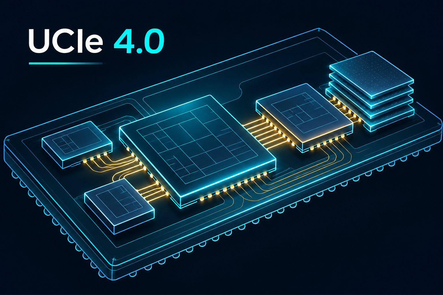
The UCIe Consortium has released the UCIe 4.0 specification, adding standardized on-package memory connectivity, power-optimized high-speed link profiles and expanded chiplet security and manageability. The latest version of Universal Chiplet Interconnect Express shifts the standard further from basic die-to-die connectivity toward comprehensive system-in-package integration for heterogeneous computing. According to the consortium, the UCIe.mem interface can achieve up to 93.75% data efficiency and approximately 2.5 TB/s/mm of die-edge bandwidth density.
UCIe.mem defines standardized connectivity between SoCs and memory logic dies inside advanced packages. UCIe 4.0 also introduces co-optimized link profiles that the consortium says provide 30% to 80% better energy efficiency, while enhanced UCIe-S bump mapping at 48 GT/s and 64 GT/s improves shoreline bandwidth density by about 20% and area bandwidth density by about 10%. The new optimizations build on the 64 GT/s signaling introduced with UCIe 3.0 rather than establishing that signaling rate for the first time.
The specification adds Trusted Reporting of Chiplet State (TRoCS), integrity-protected management channels, expanded reset-management and chiplet-state visibility, along with optional error notifications and link-health monitors for applications including automotive electronics. The consortium says the specification remains backward compatible with earlier UCIe versions. These functions address the operational requirements of multi-vendor chiplet assemblies, where connectivity must be accompanied by testing, monitoring, security and system-level control.
| UCIe 4.0 | Key Technical Advances | |
| UCIe.mem | • Standardized on-package SoC-to-memory-logic-die connectivity |
| Data efficiency | • Up to 93.75% |
| Die-edge bandwidth | • Approximately 2.5 TB/s/mm |
| Link efficiency | • Consortium reports 30–80% greater energy efficiency with co-optimized profiles |
| Enhanced UCIe-S | • 48 GT/s and 64 GT/s bump maps; approximately 20% better shoreline and 10% better area bandwidth density |
| Security | • Trusted Reporting of Chiplet State (TRoCS) and integrity-protected management channels |
| Manageability | • Expanded reset management and chiplet-state visibility |
| Reliability | • Optional error notifications and link-health monitoring, including automotive applications |
| Compatibility | • Backward compatible with previous UCIe specifications |
Analysis
The principal change is the addition of an open memory interface within the package. By specifying connections between compute and memory logic dies, UCIe.mem creates a standard option for modular memory subsystem designs that may be useful to AI accelerators and HPC processors. This does not guarantee interchangeability across all memory technologies or package implementations; that depends on the actual interfaces, integration and validation.
The stated 2.5 TB/s/mm figure represents bandwidth per unit of die edge, not aggregate memory bandwidth for a complete accelerator. Similarly, the consortium’s power-efficiency percentages describe specification-level improvements, not verified gains across every manufactured device. Actual throughput and energy consumption depend on implementation, packaging, channel geometry and operating conditions.
The security and manageability provisions extend the standard into package operations. Chiplet-state reporting, protected management communications, reset coordination and health monitoring are relevant when different suppliers contribute dies to a system. UCIe 4.0 follows UCIe 2.0’s system manageability and 3D packaging capabilities and UCIe 3.0’s higher signaling rates, preserving an evolutionary path for interoperable chiplet designs.
UCIe Specification Evolution | 2022–2026
| UCIe | The Evolution of Chiplet Standards | |
| 2022–2026 • From die-to-die interoperability to system-level chiplet integration | |
| VERSION / RELEASE | TECHNICAL MILESTONES |
| 1.0 Mar 2, 2022 Foundation | Open Die-to-Die Interconnect • Standard physical layer, protocol stack and software model • PCIe and CXL protocol support • Standard and advanced packaging models • Compliance framework for multi-vendor chiplets Key advance: Common interface for heterogeneous chiplet integration |
| 1.1 Aug 8, 2023 Refinement | Reliability and Interoperability • Simultaneous multi-protocol operation • Runtime health monitoring and repair • Automotive reliability enhancements • New bump maps for lower-cost packaging • Architecture attributes for compliance testing Key advance: Broader application support and testability |
| 2.0 Aug 6, 2024 3D Integration | 3D Packaging and Manageability • Standardized SiP management architecture • UCIe DFx Architecture for test, debug and telemetry • UCIe-3D support for hybrid bonding • Bump pitches from 10–25 µm down to 1 µm or less • 32 GT/s maximum signaling rate Key advance: Lifecycle management and stacked-die integration |
| 3.0 Aug 5, 2025 Performance | Higher Bandwidth and Control • New 48 and 64 GT/s signaling rates • Up to 2× the 2.0 maximum data rate • Sideband channel reach up to 100 mm • Continuous streaming protocol mappings • Early firmware download and priority sideband packets • Fast throttling and emergency shutdown Key advance: High-speed chiplet fabrics with expanded system controls |
| 4.0 Nov 12, 2026 LATEST RELEASE System Integration | Memory, Power and Security • UCIe.mem: standardized on-package memory links • Up to 93.75% data efficiency • Approximately 2.5 TB/s/mm die-edge bandwidth density • 30–80% better link energy efficiency with co-optimized profiles • Enhanced UCIe-S: ~20% shoreline and ~10% area bandwidth-density improvements • Trusted chiplet-state reporting (TRoCS) and integrity-protected management • Expanded reset and link-health management Key advance: Standardized memory integration and system-level chiplet control |
| ARCHITECTURAL PROGRESSION Connectivity → Reliability → 3D Integration → Performance → Memory and Security | |
| Source: UCIe Consortium specification documentation and dated press releases, 2022–2026. Published efficiency and bandwidth-density figures are specification capabilities, not universal production-device performance measurements. GT/s denotes giga-transfers per second; TB/s/mm denotes terabytes per second per millimeter of die edge. | |
| Company Profile | UCIe Consortium | |
| Organization | Universal Chiplet Interconnect Express (UCIe) Consortium |
| Location | Beaverton, Oregon, USA (contact address) |
| Structure | Industry standards consortium; Delaware nonprofit corporation |
| Standard | Universal Chiplet Interconnect Express, version 4.0 |
| Technologies | Die-to-die interconnect, advanced packaging, UCIe.mem, security and manageability |
| Markets | AI accelerators, HPC, data centers, communications and automotive |
| Website | uciexpress.org |
We’re tracking advances in chiplets, semiconductor packaging and AI infrastructure. Follow ongoing coverage at Converge Digest Semiconductors.

-
 C114 Communication Network
-
 Communication Home