Search


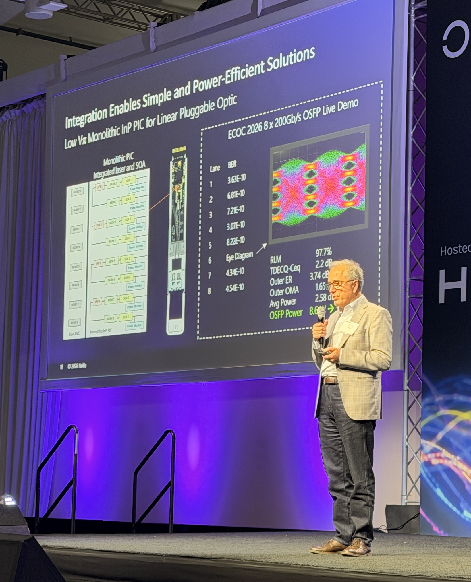
Scaling AI optical connectivity requires sustained investment in photonic integration and manufacturing capacity, alongside faster devices, according to Mehrdad Ziari, Nokia’s Senior Vice President, Optical Modules. Speaking at the PECC Summit in Sunnyvale on October 20, Ziari connected Nokia’s indium phosphide (InP) fab expansion with its work on lower-power optical modules, heterogeneous integration and simpler network deployment. He urged customers and suppliers to engage earlier, warning that manufacturing investments can require three to five years while customers may seek new capabilities within 12–18 months.
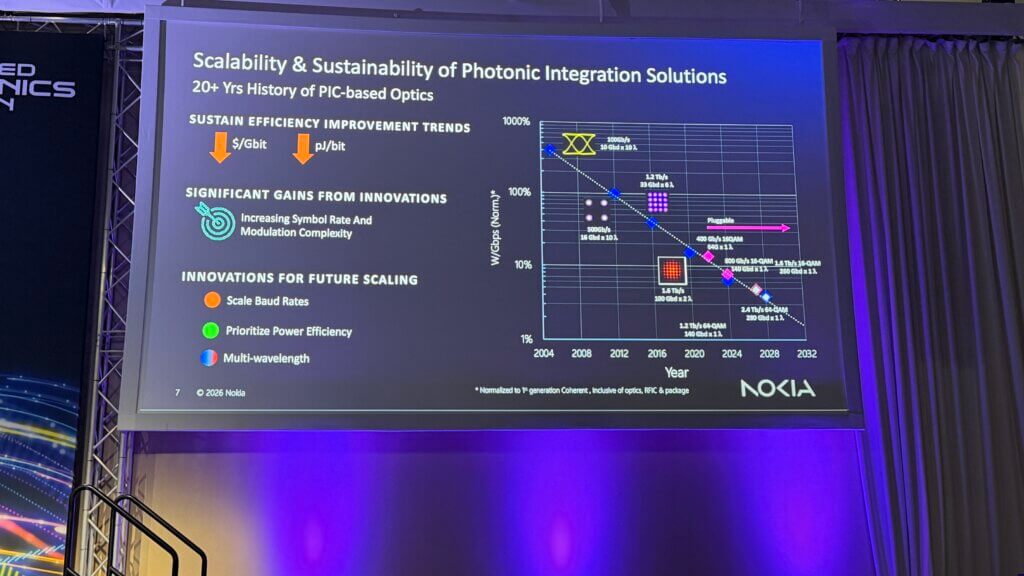
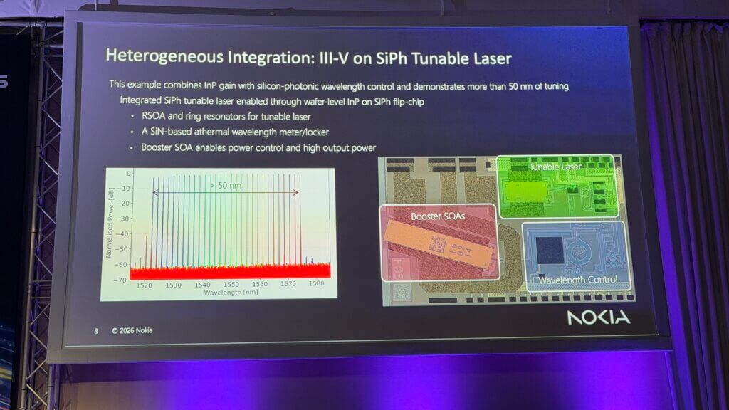
Ziari highlighted a monolithic InP photonic integrated circuit (PIC) combining four lasers, eight modulators, eight semiconductor optical amplifiers and power monitors. Nokia’s ECOC 2026 demonstration delivered eight lanes at 200 Gbps per lane in a linear pluggable optics (LPO) OSFP module consuming 8.6 W—approximately 5.4 pJ/bit at an aggregate 1.6 Tbps. He also described a heterogeneous tunable laser combining InP gain with silicon-photonic wavelength control, demonstrating more than 50 nm of tuning. Across coherent optics generations, Ziari cited an approximately tenfold improvement in power efficiency per decade, driven by photonic integration, higher symbol rates, modulation advances and system co-design; the chart also included future projections.
The manufacturing roadmap spans Nokia’s legacy Sunnyvale fab, a new six-inch InP fab in San Jose, and the planned conversion of an existing Chandler, Arizona, compound-semiconductor facility to six-inch InP production. The three facilities span 60,000, 185,000 and 1.1 million square feet, respectively—approximately 5,600, 17,200 and 102,200 square meters. These are facility footprints, rather than directly comparable production-capacity figures. Nokia’s previously disclosed Chandler agreement provides for an initial lease of manufacturing capacity from early 2027, subject to regulatory approvals, with acquisition of the full site expected in Q1 2029. Ziari said scaling also requires automated manufacturing, reliable packaging and installation processes suited to millions of optical connections.
| Nokia at PECC | Integration, Power and Production | |
| 1.6T LPO | • ECOC demonstration: 8 × 200 Gbps in OSFP; 8.6 W power consumption, equivalent to approximately 5.4 pJ/bit at 1.6 Tbps. |
| Monolithic InP | • Four lasers, eight modulators, eight SOAs and power monitors integrated on one PIC. |
| Hybrid laser | • InP gain plus silicon-photonic wavelength control; more than 50 nm tuning, with a SiN-based athermal wavelength meter/locker and booster SOA. |
| Efficiency roadmap | • Ziari cited approximately 10× improvement per decade. The chart is normalized to first-generation coherent optics and includes optics, RFIC and packaging; later points include projections. |
| Manufacturing | • San Jose: six-inch (approximately 150 mm) InP wafers. Chandler: planned conversion from six-inch GaN/SiC manufacturing to InP. |
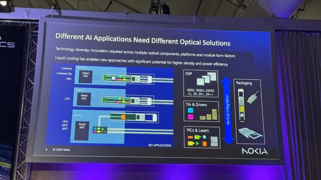
| Deployment | • Co-design, packaging, liquid cooling, reliability and simpler installation must advance alongside component performance. |
“We need to talk together more,” said Ziari, calling for earlier collaboration between customers and the optical supply chain.
Analysis
Ziari’s examples connect two distinct integration strategies. Monolithic InP combines light generation, modulation and amplification on a single photonic chip, while heterogeneous integration combines InP gain with silicon-based wavelength-control functions. His presentation treated these as complementary tools for different applications. The LPO demonstration illustrates the potential of integrated devices and linear drive to reduce module power, but the displayed result does not establish the power of a complete host-to-host link or an entire AI fabric.
Manufacturing and deployment impose separate scaling requirements. Larger facility footprints do not by themselves establish wafer output, yield or qualified module shipments, and the Chandler conversion remains a future program. Ziari’s call for earlier customer engagement reflects the mismatch between multiyear fab investment and shorter product-request cycles. His emphasis on reliability, simplified installation and AI-enabled manufacturing also broadens the discussion beyond device speed to the practical work of producing, testing and operating optical connections at volume.
| Company Profile | Nokia | |
| Company | Public company · NYSE: NOK |
| Headquarters | Espoo, Finland |
| President and CEO | Justin Hotard |
| Business | Fixed, mobile, IP, optical, data-center and network-automation infrastructure. |
| Optical capabilities | Coherent transport, pluggable optics, InP PICs, optical modules, DSPs and packaging. |
| Manufacturing focus | U.S. InP fab expansion; planned Chandler conversion and acquisition remain subject to the disclosed transaction timetable. |

-
 C114 Communication Network
-
 Communication Home