
 Search

Marvell Technology
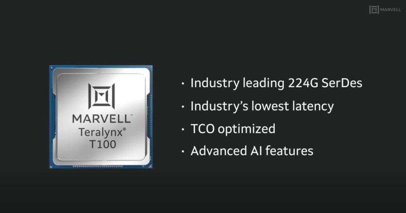
When the doors of the San Jose McEnery Convention Center open this morning at 7:30 a.m. PT (10:30 a.m. ET) for the OCP Global Summit 2026, Marvell Technology will be ready at Booth #B31 with the most expansive product showcase in the company's OCP history. At the center of that showcase sits the Teralynx T100 — industry's first 102.4 Tbps switch silicon purpose-built for AI — alongside the Structera CXL memory expansion and pooling platform designed to dismantle the memory capacity constraints now throttling frontier AI workloads. The event runs through October 15 and is sold out for the first time, a reported first for the OCP Summit.
Marvell's decision to bring nine live product demonstrations and 14 technical sessions to a single four-day event is a signal that OCP 2026 represents a strategic inflection point for open, standards-based AI infrastructure. The portfolio on the show floor — from the Teralynx T100 at the switching tier to Structera CXL at the memory tier to Bravera SC6 at the storage tier, all secured by an integrated LiquidSecurity hardware security module — constitutes what appears to be the most complete open-standards AI infrastructure portfolio from a US-based merchant-silicon vendor to date, according to Marvell's OCP showcase materials.
Teralynx T100: Industry's First 102.4 Tbps Switch Silicon
When Marvell unveiled the Teralynx T100 at Computex in June 2026, the chip became what Marvell describes as the industry's first 102.4 Tbps switch silicon purpose-built for the AI era.
Analyst Tom Hollingsworth of Futurum Group, writing on the T100's significance, argued that AI networking centers on power management rather than raw bandwidth, noting that networking can consume 15 to 25 percent of rack power as GPU racks approach 120 kW per cabinet. He also observed that Marvell enters the 102.4 Tbps segment alongside Broadcom's Tomahawk 6, where competitors have already begun shipping equivalent-class products — meaning Marvell's success will be determined by deployment wins at hyperscale customers, not specifications alone.
Architecture and Process Node
The Teralynx T100 is a monolithic device manufactured on a 3nm process, which eliminates legacy elements that would otherwise increase power and die area in competing solutions, according to Marvell's Teralynx T100 product announcement. That monolithic design choice carries architectural significance: competing switch products at similar or lower bandwidth tiers often rely on chiplet tiles or multi-die packages that add inter-die interconnect latency, power, and integration complexity. By placing a single 102.4 Tbps die on 3nm silicon, Marvell is betting that integration efficiency and AI-specific pipeline simplification — on-chip telemetry, congestion control tuned for collective AI traffic, and memory-semantic addressing support — more than compensate for the die-area risk inherent in a large monolithic device.
The 3nm process node provides the transistor density needed to embed substantial per-flow state storage and telemetry buffers on-die, which is what enables features like closed-loop congestion management and in-network telemetry at full line rate — capabilities that were computationally infeasible on 7nm equivalents without separate offload processors.
Power and Scale
According to Marvell, the T100 operates below 1,000 watts typical power, using up to 25 percent less than rival products. These figures are Marvell's own claims and have not yet been independently audited by a third party, but their implication is concrete: lower switch power allows data center operators to deploy additional accelerators within existing power envelopes rather than undertaking new facility infrastructure.
For scale-out deployments, the T100 supports up to a 512-port radix, enabling network architects to consolidate tiers and reduce latency across large AI training clusters. For scale-up deployments, a programmable pipeline architecture supports both Ethernet and emerging UALink-derived interconnect protocols. The chip also includes telemetry, congestion control tuned for AI traffic, and advanced AI traffic management capabilities.
Ecosystem Alignment
The broader Teralynx family supports the Open Compute Project's Switch Abstraction Interface (SAI) and the SONiC open-source network operating system. Compatibility with OCP SAI and SONiC is not incidental: several of Marvell's sessions this week are specifically focused on extending those open-software stacks to handle AI-fabric semantics such as memory-semantic addressing and scale-up congestion management, as detailed in Marvell's 14-session OCP schedule.
Rishi Chugh, Marvell's VP and General Manager of the Data Center Switch Business Unit, stated that the Teralynx T100 "architecture delivers significant advantages in latency, power efficiency, radix scalability and overall TCO — advantages that stem directly from its purpose-built AI design approach and are required for the continued scaling of data center infrastructure."
The T100 is currently sampling to lead hyperscale customers, with broader availability expected in early 2027.
Structera: Tearing Down Memory Wall Across Three Tiers
If the Teralynx T100 is Marvell's answer to the networking bottleneck, the Structera platform addresses an equally critical constraint: the gap between the memory capacity that large language models require at inference time and what conventional server DRAM architectures can deliver. The problem is documented across the AI industry as the "memory wall" — a scaling crisis driven by the fact that transformer model weights and KV-cache data increasingly exceed what fits in the DRAM directly attached to a GPU or CPU.
Marvell addresses the constraint across three complementary CXL product categories — making it, by the company's own account, the only vendor with a portfolio spanning all three tiers of CXL memory architecture, as described in the Structera S CXL switch press release.
Structera X — Memory Expansion
CXL memory expanders do not add processing cores; they provide raw capacity by converting PCIe slots — which exist in far greater numbers on modern servers than DIMM slots — into expanded memory resources. Up to 12 TB of memory can be added to a single processor through Marvell Structera X. The modules support both DDR4 and DDR5 and consume fewer than 30 watts per device — a low enough thermal draw to justify adding multiple units per server without materially affecting cooling budgets.
The practical impact on AI inference is concrete: Marvell's own benchmarking showed that adding 128 GB of CXL memory via a single Structera X module can accelerate inference tasks such as time-to-first-token by nearly four times. That figure is a Marvell benchmark and has not been independently reproduced, but it directionally reflects a well-documented phenomenon: LLM inference is frequently bottleneck-bound by memory bandwidth and capacity, not compute, making capacity expansion directly translatable to throughput improvement.
Structera A — Near-Memory Acceleration
Structera A adds compute to the CXL memory tier. The device features Arm Neoverse V2 cores with up to 1.6 Tbps of memory bandwidth, enabling processing logic to run directly alongside the expanded memory pool. This reduces round-trip latency to the host CPU and is particularly suited to transformer inference, where key-value cache retrieval is a dominant workload pattern.
Structera S — Rack-Level Memory Pooling
The most recently announced member of the family, the Structera S 30260, emerged from Marvell's acquisition of XConn Technologies for approximately $540 million in January 2026. The Structera S 30260 is a 260-lane CXL switch device that enables rack-level memory pooling. Working in concert with Structera A near-memory accelerators, Structera X memory-expansion controllers, and Alaska P PCIe/CXL retimers, the switch allows data center operators to access disaggregated memory resources outside the physical server — memory that no longer belongs to any single host but can be dynamically allocated across a rack of accelerators.
With CXL 3.0 support and aggregate bandwidth up to 4 TB/s, the Structera S CXL switch completes the Marvell CXL product family. At the Flash Memory Summit (FMS) 2026 in August, Marvell showed Structera S reaching 48 TB in rack-scale memory pooling.
What CXL 3.0 enables that earlier versions could not: CXL 1.x connected single devices to a single host; CXL 2.0 added switching but without bandwidth improvement; CXL 3.0, based on PCIe 6.0's 64 GT/s PAM-4 signaling, adds multi-level switching and enables multiple hosts to share a single memory pool with coherency semantics. That multi-level switching is what allows the Structera S to serve as a shared memory resource across an entire rack of GPU accelerators — a capability architecturally impossible under earlier CXL revisions.
Ara T: 1.6 Tbps Transmit-Retimed Optical DSP
Complementing the switching and memory platforms, Marvell is demonstrating the Ara T at OCP 2026 — the industry's first 8×200G transmit-retimed optics (TRO) DSP designed to reduce power and total cost of ownership in high-speed optical interconnects, according to the Ara T product portfolio announcement.
Manufactured on the same 3nm process node as the Teralynx T100, the Ara T doubles total module bandwidth to 1.6 Tbps. The direct-drive capabilities of the DSP simplify manufacturing and reduce optical module power consumption.
The key architectural distinction between transmit-retimed optics and fully retimed optics is power. In a fully retimed (FRO) design, the DSP regenerates and re-times the signal on both the transmit and receive paths — maximizing signal integrity at the cost of higher power, typically 20 to 25 watts per module. A TRO design conditions the signal only at the point of transmission, not on the receive side, improving power efficiency while preserving sufficient link budget for AI cluster interconnects. Across thousands of optical links in a large AI training cluster, that gap compounds into meaningful power infrastructure savings.
Marvell has been building toward this milestone on a multi-generation roadmap: the Ara T extends a line that began with the Nova 200G/lane DSP platform in 2023 and continued with the 3nm Ara platform in 2024. The Ara T DSP has been sampling to customers since Q1 2026.
Bravera SC6: PCIe Gen 6 SSD Controller for AI Storage
At the storage tier, Marvell is showcasing the Bravera SC6, its PCIe Gen 6 SSD controller, announced at FMS 2026 in August.
The Bravera SC6 is designed to support AI inference workloads that require frequent movement of key-value (KV) cache data between high-bandwidth memory and SSD storage — the "KV-cache spill" pattern that becomes common when an LLM's active KV-cache exceeds available DRAM. Marvell says the SC6 doubles Bravera SC5 performance from its PCIe 5.0 predecessor.
The underlying technology driver is PCIe Gen 6, which doubles per-lane throughput from 32 GT/s (Gen 5) to 64 GT/s using PAM-4 signaling with forward error correction — translating to approximately 121 GB/s over a x16 link, versus 63 GB/s for Gen 5. The Bravera SC6 supports PCIe Gen 6 and NVMe 2.2, and supports 3,600 MT/s across 16 channels from multiple suppliers. The NAND-agnostic sourcing strategy aligns with hyperscaler procurement preferences for multi-vendor flexibility. Customer sampling for the Bravera SC6 is expected to begin in Q4 2026.
Integrated Hardware Security Module
Rounding out the booth demonstrations is a new integrated hardware security module (HSM) for AI data center deployments. Marvell has deep background in silicon-level cryptographic security through its LiquidSecurity platform — the industry's first FIPS 140-2 and 140-3 Level 3 certified HSM adapters, Common Criteria, eIDAS, and PCI-PTS compliance, trusted by major cloud service providers and powered by the OCTEON DPU.
The integrated HSM shown at OCP represents the next step in that lineage: bringing key management and cryptographic offload directly into server-tray silicon, rather than requiring discrete appliance hardware. As AI workloads span thousands of accelerators and petabytes of model weights across multi-tenant hyperscale environments, the ability to anchor cryptographic trust at the hardware silicon level — with FIPS 140-3 assurance — becomes a structural security requirement, not an optional feature. Two dedicated sessions on Thursday address this security theme in technical depth.
Full Schedule: 14 Marvell Sessions at OCP 2026
Marvell's presence extends well beyond the exhibit hall. Across four days, the company's engineers and executives will contribute 14 sessions spanning AI networking software, CXL memory semantics, optical reliability, scale-up interconnects, hardware security, and custom HBM co-design.
Monday, October 12
Executive Session: "Spearheading a New Security Standard for Data Centers" | 12:50–1:10 p.m. ET | SJCC Concourse Level, Room 210CG | Cary Ussery, SVP and GM, Multimarket Business Group
The opening Marvell keynote-tier session is scheduled to kick off the week with a security-first argument for AI data center architecture. Ussery's talk will advocate for a new silicon-rooted standard for key management and cryptographic assurance in hyperscale deployments — a theme that runs through several of Marvell's contributions this week and anchors the integrated HSM product line on the show floor.
Tuesday, October 13
1. "Connectivity-Bound AI: Open Standards for Scale-Up and Scale-Out" | 1:50–2:05 p.m. ET | SJCC Concourse Level, Expo Hall Theater | Rajagopal Krishnaswamy, AVP, Product Marketing, Cloud Switch
This session will examine how open connectivity standards — Ethernet for scale-out, UALink for scale-up — can replace proprietary fabrics and give hyperscalers the deployment flexibility they are demanding. The Teralynx T100 and Marvell's UALink custom silicon will serve as the concrete anchors for the argument.
2. "Closing the Observability Loop in SAI: From Performance Telemetry to Platform Constraint Discovery" | 3:40–4:00 p.m. ET | SJCC Concourse Level, Room 210AE | Ravindranath Coimbatore Kanakarajan, Distinguished Engineer
This breakout session will examine a gap in current AI fabric operations: the inability to close the loop between per-flow telemetry captured by a switch and system-level constraint discovery. Kanakarajan will present extensions to OCP SAI that expose richer performance signals, enabling autonomous control planes to detect congestion, path failures, and hotspots more rapidly as AI training jobs scale to thousands of GPUs.
Wednesday, October 14
Wednesday is the heaviest single day for Marvell content, with five breakout sessions plus a panel, coinciding with the OCP Future Technologies Symposium.
3. "Beyond Scale-out: SONiC's Path to Memory-Semantic AI Fabrics" | 9:05–9:25 a.m. ET | SJCC Concourse Level, Room 230A | Ravindranath Coimbatore Kanakarajan, Distinguished Engineer
This session will argue that SONiC, currently deployed primarily as a scale-out control plane, must evolve to support "memory-semantic" AI fabrics — topologies where CXL or UALink switches blur the boundary between memory interconnect and packet network. The talk will outline concrete extensions to SONiC's data model and agent architecture to accommodate those requirements.
4. "Bridging Compute and Memory Fabric: Data Services for Direct XPU Access" | 12:50–1:05 p.m. ET | SJCC Lower Level, Room LL21DE | Gaurav Agarwal, Senior Distinguished Engineer
Agarwal will address one of the deeper challenges in composable memory infrastructure: enabling AI accelerators to access disaggregated CXL memory pools directly, without CPU mediation. The session will cover the addressing, coherence, and access-control abstractions necessary for safe, high-performance direct XPU-to-memory-fabric transactions — the capability that underpins the Structera S CXL switch's value proposition.
5. "Plug-and-Play ML Pipelines for SONiC: On-Device Intelligence with Advanced Feature Extraction" | 1:45–2:05 p.m. ET | SJCC Concourse Level, Room 230A | Venkata Ravichandra Mynidi, Senior Principal Engineer
This session will introduce a framework for running ML inference pipelines directly on SONiC-based network switches — without custom firmware or out-of-band servers. By embedding lightweight ML models into the switch's NPU or management plane, operators can perform real-time anomaly detection and traffic classification at line rate.
6. Panel: "Scale-Up Optical Reliability and GPU/System Resiliency to Optical Link Flaps" | 3:54–5:00 p.m. ET | SJCC Lower Level, Room LL21BC | Lenin Patra, SVP, Platform and Switch Architecture
Patra will join an industry panel on one of the most operationally sensitive topics in AI cluster design: what happens when a single optical link fails inside a scale-up fabric serving thousands of GPUs. The panel will examine detection latency, failover paths, and the topology and redundancy choices that determine whether a link flap causes a full training-job restart or a graceful degradation.
7. "Beyond the Monolith: Open Middleware for Heterogeneous AI Infrastructure at Hyperscale" | 4:35–5:00 p.m. ET | SJCC Lower Level, Room LL21DE | Gaurav Agarwal, Senior Distinguished Engineer
Agarwal returns for a second session arguing that monolithic software stacks controlling today's AI clusters will need to fragment into open, composable middleware layers as hardware heterogeneity increases. The talk will cover API boundaries, resource abstraction models, and orchestration patterns for environments where compute, memory, and network resources are supplied by different vendors connected by multiple open standards.
Thursday, October 15
8. "Integrated HSM: Bringing Silicon-Level Key Security to Server Tray" | 8:20–8:40 a.m. ET | SJCC Concourse Level, Room 212 | Craig Barner, Senior Distinguished Engineer
Barner will detail the architectural rationale for bringing HSM functionality directly into server-tray silicon, covering the trust boundary, key isolation, attestation flows, and integration with host firmware.
9. "Custom HBM as System: Co-Designing Base Die, Die-to-Die Power, and Package Thermals for AI Accelerators" | 8:20–8:40 a.m. ET | SJCC Concourse Level, Room 211 | Hsin-wei Tseng, Director, Product Management
Running concurrently with Barner's HSM session, Tseng will open the hood on Marvell's custom silicon program for AI accelerators, focusing on jointly optimizing HBM base-die architecture, die-to-die power delivery, and package thermal paths to achieve higher effective bandwidth and lower power at the system level.
10. "UALink-SAI: Common Abstraction for Scale-Up AI Switches" | 10:05–10:25 a.m. ET | SJCC Concourse Level, Room 210AE | Ayyappa Nuthalapati, Senior Principal Software Architect; Ravindranath Coimbatore Kanakarajan, Distinguished Engineer
UALink is the open industry standard for scale-up connectivity, enabling multiple AI accelerators to operate together as a single, larger system. This session will propose extending OCP's Switch Abstraction Interface — the de facto northbound API for Ethernet switches — to cover UALink-based scale-up switches as well, creating a unified software abstraction across both Ethernet and UALink.
11. "XPU Scale Composable Smart Memory Fabric" | 10:50–11:05 a.m. ET | SJCC Lower Level, Room LL21BC | Gaurav Agarwal, Senior Distinguished Engineer; Satananda Burla, Distinguished Engineer
Agarwal and Burla will present a CXL-based architecture in which memory resources are dynamically provisioned to XPUs on demand rather than statically assigned at server boot. The session covers the control-plane protocols, resource discovery mechanisms, and QoS primitives needed for composable memory at XPU scale.
12. "Secure Key Distribution Protocol for SoC Hardware Blocks" | 1:15–1:30 p.m. ET | SJCC Concourse Level, Room 212 | Craig Barner, Senior Distinguished Engineer
In his second Thursday session, Barner will present the protocol-level design for distributing cryptographic keys securely among hardware blocks within a complex SoC — an increasingly critical problem as AI processors integrate more security-sensitive functions alongside high-bandwidth data paths.
13. "SRv6 Path Steering, Packet Trimming and Telemetry" | 1:15–2:15 p.m. ET | SONiC Booth | Ravindranath C Kanakarajan, Distinguished Engineer; Jithender Reddy Kondam, Principal Software Engineer
This final Marvell session of the week moves to the SONiC Community booth for a deep dive into Segment Routing over IPv6 (SRv6) for AI data center fabrics. Kanakarajan and Kondam will cover SRv6 path steering, packet trimming for in-band telemetry without full packet mirroring, and the integration of these signals into closed-loop network management — giving operators finer control over multi-path AI fabric behavior than traditional ECMP approaches.
Context: Why Open Standards Beat Proprietary Fabric
The OCP Global Summit has long been the gathering where data center infrastructure decisions are pre-validated at the community level before they become procurement standards. This year's sold-out attendance — with participants including AMD, Arm, Broadcom, Google, HPE, Intel, Meta, Microsoft, Nvidia, and Oracle, per the official OCP 2026 agenda, under the theme Scaling Innovation for the AI Era — reflects the pace at which AI workload requirements are rewriting the rulebook for network, memory, and storage design.
What the draft agenda makes explicit is that the central infrastructure question at OCP 2026 is not whether open standards will displace proprietary AI fabrics — it is how quickly. Hyperscalers and cloud data center operators are increasingly demanding open, standards-based architectures that give them the flexibility to design AI infrastructure to meet their specific performance, power, and workload requirements without vendor lock-in.
The competitive stakes are direct. Marvell's Teralynx T100 enters the 102.4 Tbps merchant switch market alongside Broadcom's Tomahawk 6, which has already begun shipping to customers. Marvell's differentiation rests primarily on power efficiency — the under-1,000-watt typical power claim and the 3nm monolithic architecture — and on deeper native support for AI-specific pipeline functions without software adaptation. In the scale-up interconnect market, the competitive pressure is on Nvidia's proprietary NVLink: UALink, the open standard that Marvell's T100 and Thursday session explicitly support, was formed by members of the UALink founding consortium — including AMD, Intel, Google, Microsoft, Meta, Cisco, HPE, and other accelerator vendors — as a direct open alternative to NVLink's closed ecosystem. The T100's programmable pipeline support for both Ethernet (scale-out) and UALink (scale-up) is not incidental — it is a deliberate architectural bet that open standards will win, and that hyperscalers willing to standardize on open interconnects can get the same scale-up performance without committing to a single accelerator vendor's fabric.
The OCP Foundation also announced the 2027 OCP Summit moves to Moscone in downtown San Francisco — a venue upgrade that signals the event's continued expansion.
For infrastructure buyers tracking the AI silicon supply chain, the four days ahead in San Jose will provide the clearest view yet of where open AI infrastructure standards are headed — and which vendors have the silicon ready to back the promises they are making on stage.
Frequently Asked Questions
How does Marvell's Teralynx T100 differ from Broadcom's Tomahawk 6 in AI networking?
Both the Teralynx T100 and Broadcom's Tomahawk 6 operate in the 102.4 Tbps merchant switch silicon category, making Marvell and Broadcom direct competitors for hyperscale AI networking deployments. Marvell's primary differentiation arguments are power efficiency — claiming under 1,000 watts typical power and 25 percent less than rival products, though these figures have not yet been independently audited — and a monolithic 3nm die architecture that eliminates the inter-die interconnect overhead present in multi-die chiplet designs. Marvell also argues that the T100's pipeline was designed from scratch for AI traffic patterns, including native congestion control for collective communication operations. Whether these architectural differences translate into deployment wins will be determined by hyperscale customer evaluation programs currently underway.
What is CXL, and how does Structera solve the AI memory wall?
Compute Express Link (CXL) is an open-standard interconnect, built on the PCIe physical layer, that allows additional memory capacity and compute-adjacent memory resources to attach to a server through PCIe slots rather than the more limited DIMM slots used for conventional DRAM. The "memory wall" in AI inference refers to the gap between the memory capacity that large language models require for their weights and KV-cache, and what physically fits in a server's DRAM. Marvell's Structera platform addresses this gap across three CXL tiers: Structera X adds raw capacity (up to 12 TB per processor), Structera A adds near-memory compute with Arm Neoverse V2 cores, and Structera S provides a 260-lane CXL 3.0 switch that enables up to 48 TB of memory to be pooled and shared at rack scale across multiple AI accelerators. CXL 3.0 specifically — which Structera S implements — enables multi-level switching and memory sharing across multiple hosts, a capability not available in CXL 1.x or 2.0.
When will Teralynx T100 be commercially available, and who can access it now?
As of OCP Summit 2026, the Teralynx T100 is sampling to lead hyperscale customers — meaning a small number of major cloud providers are already evaluating the chip in their infrastructure environments. Broad commercial availability is targeted for early 2027. The Ara T optical DSP has been sampling since Q1 2026. The Bravera SC6 PCIe Gen 6 SSD controller is scheduled to begin customer sampling in Q4 2026. Organizations not in Marvell's lead-customer program should plan for evaluation access beginning in early 2027 for the T100 and late Q4 2026 for the SC6.
What is UALink, and how does it challenge Nvidia's NVLink scale-up interconnect?
UALink (Ultra Accelerator Link) is an open industry standard specifically designed for scale-up AI interconnects — the high-speed, low-latency fabric that allows multiple AI accelerators to communicate directly with each other during training and collective operations like all-reduce. UALink was developed by a consortium that includes AMD, Intel, Google, Microsoft, Meta, Cisco, HPE, and other accelerator vendors specifically as an open alternative to Nvidia's NVLink, which is a proprietary interconnect available only to customers using Nvidia accelerators. Because NVLink is proprietary, operators who build their AI training clusters around it become dependent on Nvidia for their entire scale-up networking layer. UALink's 1.0 specification has been finalized. Marvell's Teralynx T100 supports both Ethernet (scale-out) and UALink-derived protocols (scale-up) through its programmable pipeline, and Thursday's session at OCP 2026 proposes extending the OCP Switch Abstraction Interface to cover UALink switches — a move that would make UALink a first-class, vendor-neutral, software-managed interconnect alongside Ethernet.

-
 C114 Communication Network
 -
 Communication Home
