
 Search

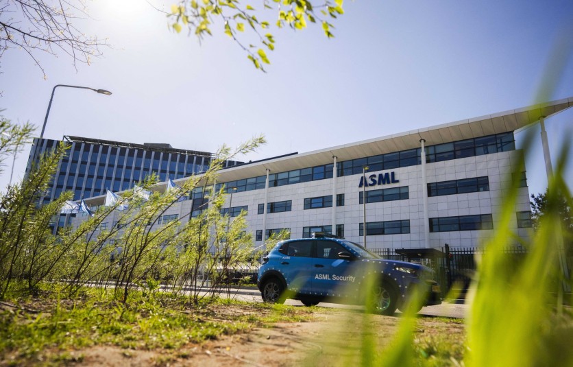
A private security vehicle drives outside Dutch tech giant ASML's corporate headquarters in Veldhoven during its general shareholders' meeting on April 22, 2026. Freek VAN DEN BERGH/ANP / AFP via Getty Images
The world's only manufacturer of advanced chip-printing machines crossed a production-readiness milestone last week that its customers had been watching closely: ten High-NA extreme ultraviolet lithography systems are now operating at four chipmakers worldwide, with three more in shipment or installation, and ASML is targeting 90% fleet availability by Q4 of 2026 — the threshold customers have required for high-volume manufacturing deployment. That figure — disclosed by ASML Senior Vice President Greet Storms at SEMICON Taiwan — arrived the same week ASML broke ground on its second major industrial campus in the Netherlands, the physical infrastructure bet that backs up four simultaneous chipmaker commitments to a machine priced at roughly $380 to $400 million per unit.
The simultaneous arrival of those two data points — a fleet reaching production scale and a factory being built to produce more of them — frames the moment more precisely than either data point alone. TSMC, Samsung, SK Hynix, and Intel have all now committed to High-NA EUV, and ASML has now broken ground on the campus it will need to build enough of the machines to supply them.
Why ASML Is Building a Second Campus in Eindhoven
On September 8, 2026, ASML marked the start of construction of Brainport Industries Campus North (BIC North) in Eindhoven, the Netherlands, roughly 7 kilometers (4.3 miles) from its existing Veldhoven headquarters, near Eindhoven Airport. Dutch Prime Minister Rob Jetten, his predecessor Dick Schoof, and Eindhoven Mayor Jeroen Dijsselbloem attended the groundbreaking ceremony alongside representatives from government, customers, suppliers, and regional partners.
The development is planned in phases and will eventually span approximately 350,000 square meters (3,767,360 square feet), with potential capacity for up to 20,000 workplaces. The first phase, expected to complete in 2029, will house at least 3,000 employees and bring production, logistics, and office functions together in a single integrated campus.
The core of that first phase is a new "flow factory" — ASML's term for what the company describes as its next-generation TWINSCAN factory model, designed to enable faster, more efficient, and higher-scale module production. The flow factory borrows concepts from automotive and aerospace manufacturing — specifically the idea of streamlining the movement of materials and work through a production sequence to improve throughput without sacrificing precision. Applying that model to the TWINSCAN EXE:5200B, a machine that requires molybdenum-silicon multilayer mirrors in vacuum, a tin plasma generated roughly 50,000 times per second, and components assembled to sub-nanometer tolerances, is an unusual engineering challenge for a manufacturing methodology that originated in industries where tolerances are measured in millimeters, not angstroms.
ASML's existing facilities in Veldhoven are sold out. The company has planned to ship more than 60 EUV systems in 2026, including 10 High-NA EUV scanners at approximately $380 to $400 million each, with 56 low-NA, 10 High-NA in 2027. That output is not meeting demand. Standard NXE-series EUV systems — the lower-NA generation priced at roughly $200 million each — are sold out through the end of 2027. BIC North is, in the most direct sense, ASML's answer to the question of where the next generation of machines will be built.
Read more: ASML Raises Full-Year Guidance as Intel Ships First High-NA EUV Logic Chip
What Chipmakers Are Now Betting On
TSMC, the Taiwan-based foundry that manufactures chips for Apple, Nvidia, and dozens of other companies at the center of the AI hardware buildout, has committed to deploying High-NA EUV in volume production starting in 2030. That commitment represents a shift from a posture of open skepticism: TSMC had previously questioned whether the economics of High-NA justified the cost over its existing process optimization strategies. The company's stated rationale for the reversal is increasingly complex transistor architectures required for AI applications — a signal that no amount of packaging innovation will ultimately substitute for finer lithography at the leading edge. The ASML and TSMC joint initiative also targets a 12-inch photomask pilot line by 2031 and full High-NA lithography system readiness for advanced-node production by 2033.
Samsung has moved more aggressively. The company announced an enhanced strategic partnership with ASML on September 8, 2026, targeting High-NA EUV for high-volume DRAM manufacturing by 2028 — ahead of any 12-inch photomask availability, meaning it will begin production using 6-inch masks with stitching in the interim. Samsung CEO Jun Young-hyun framed the commitment explicitly in AI terms, stating that the AI era requires technological innovation across the entire chip value chain.
SK Hynix has separately confirmed a 2028 High-NA EUV target for its own memory operations, joining Samsung in targeting DRAM production — a category that reaches the break-even point for High-NA economics earlier than logic chips because DRAM dies are smaller, making the multi-patterning reduction benefits tip the cost-per-wafer math sooner.
Intel stands apart from its peers as the only chipmaker that has already crossed the production threshold. The company's High-NA systems, which it began installing in 2024, have now processed more than 1.35 million wafers — up from the one million reported at the SPIE BACUS conference in September 2026 — across development, qualification, and volume production on select layers of its Core Ultra Series 3 Panther Lake processors, built on Intel's 18A process node.
How the Technology Actually Works — and What Makes It Expensive
A standard EUV scanner — the TWINSCAN NXE series, which runs at 0.33 numerical aperture — works by generating 13.5-nanometer extreme ultraviolet light from a tin plasma. A CO₂ laser fires at molten tin droplets roughly 50,000 times per second; the resulting plasma emits EUV light that is collected by a mirror, directed through a series of molybdenum-silicon multilayer mirrors operating in high vacuum, and focused through a photomask onto a silicon wafer coated in photoresist. Because all matter absorbs EUV radiation, the entire optical path must operate in near-vacuum, and each of the machine's approximately eleven mirrors absorbs roughly 30% of the incident light — meaning only about 2% of the light generated by the source reaches the wafer.
High-NA EUV, sold by ASML as the TWINSCAN EXE:5200B, raises the numerical aperture from 0.33 to 0.55. Higher numerical aperture directly improves achievable resolution under the Rayleigh criterion: the EXE:5200B achieves 8-nanometer resolution compared to roughly 13 nanometers for standard EUV, with approximately 40% greater imaging contrast. In practical terms, features can be printed approximately 1.7 times smaller per exposure, enabling transistor densities roughly three times higher.
The jump in optical performance is not free. Increasing the numerical aperture to 0.55 required ASML engineers to adopt an anamorphic optical design — one that demagnifies the photomask pattern differently in the horizontal and vertical directions. Standard EUV scanners apply uniform 4× magnification reduction in both directions, producing an exposure field on the wafer of 26 mm × 33 mm (1.02 in × 1.30 in). The High-NA system uses 4× horizontal and 8× vertical demagnification, which halves the exposure field in the scanning direction to 26 mm × 16.5 mm (1.02 in × 0.65 in).
That halved field is not a firmware setting — it is a physical consequence of the laws of optics. For chip dies smaller than the new field size, the reduction is irrelevant. For the large-die AI accelerators that are now the semiconductor industry's most commercially important products, it creates a throughput penalty: the die must be exposed in two half-field passes, stitched together with sub-nanometer alignment accuracy. Intel presented data at the SPIE BACUS conference showing that stitching cuts High-NA throughput 30% — from approximately 175 wafers per hour to around 125 — on machines costing up to $400 million each. The 12-inch photomask initiative formed by TSMC, ASML, Samsung, and Intel on September 8 is specifically designed to eliminate that stitching penalty by 2033.
ASML's Market Position: No Competition at the Frontier
According to JPMorgan estimates, ASML held approximately 94% of the global lithography market in 2025. At the leading edge, that figure represents a complete monopoly: no other company sells EUV systems capable of manufacturing the most advanced commercial chips. Japan's Nikon and Canon produce deep ultraviolet lithography tools — an older technology generation that cannot replicate EUV's resolution at advanced nodes. Morningstar analyst Javier Correonero has characterized suggestions that Chinese competitors are close to closing the EUV technology gap as "misinformation."
The export control environment reinforces that position. Since 2019, the Netherlands government — under pressure from Washington — has restricted the export of EUV systems to China. ASML cannot sell its most advanced tools to any Chinese customer, which means the High-NA adoption wave taking place across Taiwan, South Korea, the United States, and potentially Japan is structurally inaccessible to China's semiconductor industry under current regulations.
ASML's global fleet of 314 EUV machines — all 0.33 NA models — is concentrated in Taiwan, South Korea, and the United States. The ten High-NA systems now operating across four customers are the beginning of a separate fleet requiring substantially more machines, one that ASML will need to produce in materially larger quantities to serve four simultaneous chipmaker timelines between now and 2030.
Read more: TSMC, Samsung, and Intel Back 12-Inch Photomask Standard to End 30% High-NA EUV Throughput Loss
What the Flow Factory Has to Actually Accomplish
ASML has framed BIC North in terms of growth — an additional 20,000 workplaces, production and logistics consolidated in a single campus, close proximity to its existing Veldhoven headquarters. But the number the campus will ultimately be judged by is simpler: how many EXE:5200 units can ASML produce per year, and at what reliability?
The 2026 High-NA EUV target is 10 units shipped. That number will need to grow substantially before TSMC can reach 2030 readiness, Samsung and SK Hynix can reach their 2028 DRAM targets, and Intel can complete the 14A deployment it has been engineering High-NA EUV into from the ground up. Each of those timelines implies additional machine orders 12 to 18 months in advance of the production date.
ASML CEO Christophe Fouquet, speaking at the BIC North groundbreaking ceremony, attributed the expansion directly to the AI-driven demand surge, stating that the growing global demand from the semiconductor industry requires continuous investments. Speaking separately to Reuters, Fouquet described the AI demand cycle in terms that suggest ASML is not treating this as a temporary boom: "I don't think we're at the end of it, to be honest."
The EXE:5200B's current throughput trajectory offers a preview of what the flow factory will need to sustain. ASML VP Greet Storms disclosed at SEMICON Taiwan that the fleet's availability reached 84% in July 2026, with a target of 90% availability by Q4 2026 — the minimum required for customers to commit to production use at scale. ASML's roadmap projects further throughput improvements through successive model generations: the EXE:5200C targets 160 WPH in AB mode, the EXE:5200D targets 175 WPH, and the EXE:5400E targets 180 WPH by the end of the decade, with a High Productivity EXE:5600 planned for more than 250 WPH on a timeline not yet publicly disclosed.
The gap between where the fleet is now — 10 systems, 84% availability in July, 135 WPH in acceptance testing — and where it needs to be for four simultaneous chipmaker timelines in 2028 and 2030 is the gap the flow factory campus is designed to close.
Does This Matter If You're Not in the Chip Industry?
The short answer is yes, with a lag. The chips that will eventually be manufactured using High-NA EUV at sub-2-nanometer nodes — the AI accelerators, advanced logic processors, and next-generation memory devices on the TSMC, Samsung, and SK Hynix roadmaps — are the components that will power the next generation of AI infrastructure. ASML VP Storms noted at SEMICON Taiwan that High-NA EUV supports five DRAM generations, extending its relevance in memory scaling beyond the current generation.
TSMC made the same connection explicitly: the company stated that growing AI application complexity is the primary driver behind its expectation that the number of High-NA EUV layers per device will rise through the 2030s. The timeline for when that reaches consumers — as AI tools, as devices, as cloud services — runs from TSMC's 2030 production entry through the years that follow. The groundbreaking in Eindhoven is part of that supply chain.
Frequently Asked Questions
What does "production threshold" mean for High-NA EUV, and why does 90% fleet availability matter?
In semiconductor manufacturing, a tool's "availability" measures the percentage of time it is operational and producing good wafers, rather than undergoing maintenance or experiencing downtime. For a machine as complex as ASML's High-NA EUV scanner — which requires laser-driven tin plasma generation, near-vacuum optical systems, and alignment tolerances measured at the atomic scale — reaching 90% availability is a meaningful engineering milestone. Customers building production processes around the tool need confidence that it will run reliably enough to meet yield and cost targets at volume. The EXE:5200B reached 84% availability in July 2026, with ASML targeting 90% by the end of the fourth quarter, which ASML has described as the threshold customers require for high-volume manufacturing deployment.
What is a "flow factory," and why is it unusual for semiconductor equipment manufacturing?
A flow factory is a manufacturing model — borrowed from automotive and aerospace industries — in which materials and work move continuously through a production sequence in a streamlined, synchronized way, rather than batching at individual stations. ASML has described BIC North's flow factory as its next-generation TWINSCAN manufacturing model designed to enable faster, more efficient, and higher-scale module production. The unusual aspect is the object being manufactured: a TWINSCAN EXE:5200B weighs roughly 150 to 200 tonnes and requires optical components ground to sub-nanometer specifications, tin plasma generated at 50,000 pulses per second, and assembly in conditions precise enough that the machine itself must operate in near-vacuum. Automotive flow manufacturing typically involves tolerances measured in millimeters; ASML is attempting to apply the same throughput logic to equipment assembled at the scale of atomic layers. Whether the model will deliver the productivity gains ASML needs to meet its customers' 2028 and 2030 production timelines is the central operational question the campus is designed to answer.
Why did TSMC change its position on High-NA EUV, and what does that mean for chipmakers building on TSMC's nodes?
TSMC had been openly skeptical of High-NA EUV on cost grounds: each High-NA exposure costs approximately 2.5 times more than a standard EUV exposure, and the tool costs roughly double. At TSMC's production scale, that math previously did not favor High-NA for its first sub-2-nanometer generation. TSMC's reversal reflects a conclusion that increasingly complex transistor architectures required for AI applications will eventually demand the finer patterning that only High-NA EUV can provide, as stated in TSMC's 2030 HVM commitment. For companies like Apple, Nvidia, AMD, and Qualcomm that design chips fabricated at TSMC — and whose products will be built on the nodes TSMC is roadmapping for the 2030s — TSMC's adoption timeline sets the outer boundary for when High-NA EUV-enabled performance improvements reach their products.
Is there any company that could compete with ASML on High-NA EUV?
Not commercially, and not within any near-term timeframe that matters for the current chipmaker commitments. Nikon and Canon abandoned EUV development and did not gain access to the patent pool from the EUV LLC consortium that ASML effectively inherited through its 2001 acquisition of Silicon Valley Group. China's semiconductor industry, which would be the most commercially significant potential entrant, is blocked from purchasing ASML EUV tools under Dutch and US export controls enforced since 2019. Reuters reported in December 2025 that Chinese researchers built an EUV prototype in Shenzhen — assembled by former ASML engineers — that was generating extreme ultraviolet light but had not yet produced working chips. Independent analysts estimated that if development proceeds on schedule, China could be producing functional advanced chips using domestic EUV technology by 2028 to 2030 — roughly five years behind the current state of the art. Morningstar analyst Javier Correonero has characterized broader claims about Chinese competitors closing the EUV gap as "misinformation." For the chipmakers that signed commitments to ASML's High-NA EUV in September 2026, no viable alternative exists through 2030 and beyond.

-
 C114 Communication Network
 -
 Communication Home
