
 Search

Scaleflux.com
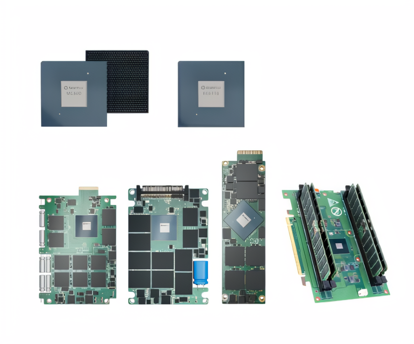
Storage and memory controller specialist ScaleFlux has announced two PCIe Gen 6 silicon products — the FC6116 NVMe SSD controller and the MC600 CXL 3.2 Type 3 memory controller — ahead of the Future of Memory and Storage (FMS) 2026 conference, which opens August 4 at the Santa Clara Convention Center. The dual announcement arrives as the Gen 6 storage transition moves from roadmap to production reality: Micron shipped the first Gen 6 SSD (the 9650) in February 2026, and Samsung entered PM1763 mass production on July 8, giving OEM engineers their first real choice of Gen 6 controller silicon to evaluate. ScaleFlux CEO Hao Zhong is scheduled to keynote FMS alongside NVIDIA's VP of Storage Technology, Jason Hardy, on August 5 — a pairing that signals how thoroughly AI compute and storage infrastructure have converged into a single design discipline.
The two products together position ScaleFlux at both ends of the AI storage bottleneck. The FC6116 maximizes how fast data reaches the GPU through the storage interface. The MC600 expands how much memory a server can carry while keeping that expanded pool coherent and low-latency through the Compute Express Link fabric. Neither product is shipping yet — FC6116 will begin sampling with key customers in the fourth quarter of 2026 — but the simultaneous Gen 6 and CXL 3.2 commitment signals that ScaleFlux intends to compete across the full memory-storage hierarchy as that hierarchy is being rebuilt for AI.
PCIe Gen 6 Doubles Storage Bandwidth by Changing How Data Is Encoded
Understanding why PCIe Gen 6 matters — and where its tradeoffs lie — requires understanding the signaling change at its core. Previous PCIe generations used NRZ (Non-Return-to-Zero) signaling: a binary scheme in which each clock cycle carries either a one or a zero. The PCIe 6.0 specification replaces NRZ with PAM-4 (Pulse Amplitude Modulation 4-level), a scheme that assigns four distinct voltage levels to each clock cycle, allowing each cycle to carry two bits instead of one, as TechInsights explains. At the same clock frequency as Gen 5, Gen 6 therefore doubles the raw data rate from 32 GT/s to 64 GT/s per lane — and for a standard x4 SSD link, that translates to a theoretical bandwidth ceiling of roughly 32 GB/s in each direction, up from approximately 16 GB/s under Gen 5.
The catch is signal integrity. PAM-4's four closely spaced voltage levels produce a significantly lower noise margin than NRZ's two levels: where NRZ creates a single large "eye" in signal analysis, PAM-4 creates three smaller eyes, each roughly one-third the height of the NRZ eye, making the link far more sensitive to jitter, channel loss, and interference, as engineering analyses of PCIe Gen 6 board design detail. To compensate, PCIe Gen 6 introduces Forward Error Correction (FEC) for the first time in the specification's history, paired with a mandatory shift to FLIT (Flow Control Unit) mode, which restructures transactions into fixed 256-byte packets rather than the variable-length packets of prior generations. This fixed-packet structure allows FEC to operate on well-defined boundaries and actually improves bandwidth efficiency for small payloads relative to Gen 5.
What the draft announcement does not address — but that infrastructure architects should factor into their evaluations — is the latency overhead that FEC introduces. Engineering analyses of PCIe Gen 6 board design put the FEC contribution at roughly 4 to 8 nanoseconds per direction. For throughput-dominant AI workloads — loading training datasets, staging model weights, writing checkpoints — this overhead is negligible against the substantial bandwidth gain. For latency-sensitive inference pipelines where NVMe round-trip time directly affects time-to-first-token generation, the FEC penalty deserves explicit consideration before assuming Gen 6 always outperforms a well-tuned Gen 5 implementation. ScaleFlux's FC6116 is clearly optimized for throughput, and its performance targets reflect that priority.
The FC6116 is designed to reach 28 GB/s sequential reads and 25 GB/s sequential writes, saturating approximately 87 percent of the Gen 6 x4 theoretical envelope — a figure that aligns with what Micron's 9650 has demonstrated in production. Random performance targets are 7 million IOPS for 4K reads and more than 1 million sustained IOPS for 4K writes. The controller supports TLC, QLC, and SLC NAND with a maximum capacity ceiling of 256 TB, and accommodates all major EDSFF form factors: E1.S/L, E3.S/L, and U.2/U.3. Active controller power is rated at under 9 watts.
Read more: Two-Phase Cooling Squeezes Dual 600W GPUs Into 1U Edge AI Server at AMD EPYC 9006 Venice Launch
FC6116 Security Architecture Goes Beyond Standard Drive Encryption
Security is treated as a first-class design requirement in the FC6116, not a checkbox. The controller supports PCIe Integrity and Data Encryption (IDE), which authenticates and encrypts the PCIe link itself — addressing supply-chain and firmware-integrity concerns that are increasingly central to hyperscale security posture, as detailed in ScaleFlux's security feature list. OCP Caliptra 2.0 compliance provides open-source root-of-trust attestation: a cryptographically verifiable chain from silicon manufacturing through firmware loading, enabling zero-trust data center architectures to verify controller integrity without trusting proprietary vendor attestation alone. CNSA 2.0 post-quantum cryptography support prepares the controller for environments where quantum-resistant key exchange is becoming a procurement requirement. TCG Opal 2.0 handles at-rest encryption, and ScaleFlux's own S.A.F.E. framework layers in additional security primitives. Compliance with the OCP Datacenter NVMe SSD Specification means FC6116 should integrate into Open Compute Project-aligned hyperscale deployments without custom work — a practical prerequisite for consideration by the largest cloud operators.
The firmware platform is Arm-based and delivered as a turnkey solution, including production-ready firmware and validated reference designs. For OEM-scale SSD makers, the significance of the turnkey approach is primarily economic: developing and qualifying enterprise NVMe firmware from scratch typically consumes 18 to 24 months of engineering time. By delivering validated firmware with customization options, ScaleFlux compresses that timeline, enabling smaller OEMs to compete in market segments that would otherwise require resources comparable to Samsung or Seagate to enter.
MC600: CXL 3.2 Controller That Speaks Both DDR Generations Simultaneously
The MC600 is ScaleFlux's entry into CXL 3.2, the most recent revision of the Compute Express Link memory interconnect standard — released by the CXL Consortium in December 2024 — which optimizes memory device monitoring, extends OS-level functionality for CXL memory devices, and adds Trusted Security Protocol support. It is built on a PCIe Gen 6 x8 physical layer and operates as a Type 3 CXL device, meaning it functions purely as a memory expander, providing the host processor with cache-coherent access to attached DRAM through the CXL.mem protocol's load/store interface. No accelerator function, no separate cache domain — the MC600 adds memory capacity to the host's address space and keeps it coherent.
Its standout architectural feature is simultaneous native support for both DDR4 and DDR5 on a single controller die: a quad-channel DDR5 (40-bit with 2DPC support) path capable of up to 2 TB, and a dual-channel DDR4 (72-bit with 2DPC support) path on the same controller. This is not a switchable configuration — the controller can interface with both memory generations in the same deployment, a capability that addresses one of the most practical constraints facing large data center operators considering CXL memory expansion.
Hyperscalers and large enterprise operators carry substantial DDR4 infrastructure in deployed servers. DDR5 offers higher bandwidth — running at 4,800 MT/s versus DDR4's 3,200 MT/s — but a transition that requires replacing all existing DRAM simultaneously imposes capital costs and operational disruption at scale that few organizations will accept. An MC600-based CXL module lets an operator add memory capacity using whichever DRAM generation makes sense for the procurement cycle, extending the ROI of existing DDR4 infrastructure while enabling a forward migration to DDR5 without a forklift upgrade. That is a meaningfully different value proposition from controllers that support only DDR5, and it reflects a similar philosophy ScaleFlux applied to its predecessor, the MC500, which was the first Type 3 CXL 3.1 controller with DDR4/DDR5 dual support when it was introduced in October 2024.
The sub-9W power budget at a PCIe Gen 6 x8 configuration is the other headline specification, and it matters for the same reason it matters in the FC6116: high-density AI server racks are already running at or near thermal limits from GPU power walls. A CXL memory expansion controller that adds meaningful DRAM capacity without proportionally increasing cooling load gives architects budget headroom they would not have with a higher-wattage solution. The MC600's security architecture mirrors the FC6116's: PCIe IDE, OCP Caliptra 2.0, S.A.F.E. framework, and firmware attestation. Form factor support spans PCIe add-in cards (AICs), EDSFF E3.S (both 1T and 2T), and custom configurations, giving OEM module partners latitude to target a range of server designs.
How the CXL Market Got Here and Where It Is Going
The broader CXL memory expansion market was valued at approximately $1.3 billion in 2025 and is projected to reach $11.8 billion by 2034, at a compound annual growth rate of around 28.7 percent, according to Mordor Intelligence (paywalled). The AI-specific segment of CXL memory expansion is estimated at approximately $740 million in 2026 and growing toward $2.79 billion by 2031 at roughly 30 percent annually. The growth is not purely speculative: Samsung and SK Hynix are both targeting CXL 3.2-compatible memory module production before the end of 2026, and controller silicon is the layer that enables those modules to function as usable infrastructure. ScaleFlux's MC600, which targets CXL 3.2 compliance, is positioned as the controller layer for that incoming wave of DRAM modules.
It is worth noting the live architectural debate that surrounds CXL's role in AI infrastructure. A widely circulated SemiAnalysis analysis from early 2024 argued that Compute Express Link's dependence on the PCIe physical layer creates a latency disadvantage against next-generation Ethernet-based fabrics for GPU memory interconnects, and that NVIDIA's NVLink architecture effectively addresses GPU memory pooling in ways that reduce CXL's relevance for that specific use case. The counter-argument from the CXL Consortium and from multiple controller vendors — and the argument that drives products like MC600 — is that CXL's value for CPU-attached memory expansion is structurally different from GPU memory pooling: it provides cache-coherent load/store semantics that Ethernet cannot offer, and it serves a persistent architectural need for expanding server main memory beyond socket capacity limits that no alternative currently addresses for CPU-attached workloads. MC600 enters that market context, not a settled one.
On the enterprise SSD demand side, McKinsey has projected 35 percent annual growth in enterprise SSD capacity demand, from 181 exabytes (EB) in 2024 to over 1,000 EB by 2030, with AI workloads as the primary driver. Whether those figures prove accurate at that precision, the directional trend is well-supported across industry sources and is evident in the accelerating product cadence from Micron, Samsung, SK Hynix, Phison, and now ScaleFlux.
ScaleFlux's Platform Progression and What It Means at FMS 2026
ScaleFlux has been building toward this announcement in deliberate steps. The company introduced computational storage drives beginning with its CSD 1000 in 2018 and developed its first fully in-house SSD controller (the SFX 3016) in 2022. In October 2024, it moved to PCIe Gen 5 with the FX5016 SSD controller and introduced three new SoCs, including the MC500 — the first Type 3 CXL 3.1 controller with simultaneous DDR4 and DDR5 support — as detailed in the October 2024 ScaleFlux announcement. At FMS 2025 in August, it demonstrated the MC500 in a CXL 3.1 interoperability test at FMS 2025 alongside XConn's switch and with AMD's public acknowledgment of ecosystem readiness. The FC6116 and MC600 represent the jump to Gen 6 — keeping the dual-DDR philosophy while advancing to the CXL 3.2 specification and the PCIe 6.0 physical layer across both products.
The competitive context at FMS 2026 is acute. Micron's 9650 has had a roughly five-month head start in the market since reaching mass production in February. Samsung's PM1763 entered mass production on July 8, using a 9th-generation V-NAND and a 4-nanometer controller, with a 28,400 MB/s sequential read ceiling and 6.92 million IOPS random read — positioned for next-generation AI platforms, as confirmed by the Samsung Semiconductor press release. Both of those products are in the hands of customers now. ScaleFlux's FC6116 will not begin sampling until the fourth quarter of 2026, placing its customers on track to enter qualification in early 2027 at the earliest — typically a 12- to 18-month process before drives reach production. That lag is a real competitive constraint against Micron's first-mover position, though it falls within the normal design-cycle window for OEMs building platforms that will not ship until 2027 or 2028.
What ScaleFlux offers alongside the silicon — validated firmware, reference designs, and contract manufacturing partner support — is the turnkey argument for OEM engineers who would otherwise spend the better part of two years building their own firmware stack before a single drive ships. That model has served the company through three controller generations and is how a Milpitas-based specialist can compete in a market where Samsung and Micron invest billions annually in their own controller development.
What Engineers Should Evaluate Before FMS Begins
Several technical questions will be clarified during and after FMS 2026, and engineers planning evaluations should put them on their watchlist.
The first is power efficiency under real AI workloads. ScaleFlux's under-9W claim for both FC6116 and MC600 is a typical-power figure — standard industry practice — and performance under sustained AI inference loads, which stress controllers differently than throughput benchmarks, will require independent verification once samples are available. For reference, Samsung notes that the PM1763's Gen 6 controller architecture achieves 1.8 times better power efficiency than its Gen 5 predecessor PM1753, setting a comparable benchmark for the category.
The second is CXL 3.2 ecosystem interoperability. Samsung and SK Hynix are targeting CXL 3.2 memory module production before year's end. MC600's value as a controller for those modules depends on validated interoperability with both the DRAM vendors' modules and with the CPU platforms — AMD EPYC Venice and Intel's next-generation Xeon both bring native PCIe Gen 6 and CXL support — that will host them in production. ScaleFlux demonstrated MC500 interoperability at FMS 2025; MC600 demonstrations at FMS 2026 would be the next validation signal to watch.
The third is the qualification timeline pressure on FC6116 customers. OEMs who design drives around FC6116 will target sampling entry in Q4 2026. Production qualification at hyperscale volume typically takes 12 to 18 months from first samples. That puts commercial product availability from FC6116-based drives in mid-to-late 2027 at the earliest — after which both Micron's and Samsung's Gen 6 offerings will have had 12 to 18 months in the market. The competitive case for FC6116 depends on differentiation that goes beyond matching the raw throughput ceiling: the turnkey platform, the dual-port 2×2 configuration support, and the post-quantum security stack are the angles where ScaleFlux can offer something Micron's 9650-era controller architecture does not.
Frequently Asked Questions
What is the difference between PCIe Gen 6 and Gen 5 for NVMe SSDs?
PCIe Gen 6 doubles the per-lane signaling rate from 32 GT/s to 64 GT/s by switching from NRZ binary signaling to PAM-4 (Pulse Amplitude Modulation 4-level), which encodes two bits per clock cycle instead of one. For a standard x4 NVMe SSD link, this roughly doubles the theoretical bandwidth ceiling from about 16 GB/s under Gen 5 to about 32 GB/s under Gen 6. The tradeoff is increased signal integrity complexity — PAM-4 has a lower noise margin than NRZ — which requires forward error correction (FEC) in Gen 6 for the first time in PCIe history. For bulk AI workloads like training data loading and model staging, Gen 6 provides a clear throughput advantage. For latency-sensitive inference pipelines, the FEC overhead (roughly 4 to 8 nanoseconds per direction) should be factored into evaluation before assuming Gen 6 is always preferable.
What does a CXL Type 3 memory controller actually do in an AI server?
A Type 3 CXL controller — like the MC600 — adds DRAM capacity to a server's memory address space beyond what the processor's native DIMM slots can hold, without requiring the processor to have direct knowledge of each memory module. The CPU accesses this expanded memory through the CXL.mem protocol using standard load/store instructions, and the CXL interconnect maintains cache coherence with local processor memory. For large language model inference, where KV cache sizes can exhaust even fully populated DDR5 configurations, CXL memory expansion lets operators increase effective memory capacity while keeping it coherent and addressable without adding a second compute socket. The MC600 specifically bridges DDR4 and DDR5 on the same controller, so operators can use whichever DRAM generation makes sense for their infrastructure budget without swapping controllers.
When will PCIe Gen 6 NVMe SSDs actually be available to buy?
Micron's 9650 entered mass production in February 2026 and is available to enterprise customers now, making it the first commercial PCIe Gen 6 SSD in the market. Samsung followed with the PM1763, which entered mass production on July 8, 2026. SK Hynix has confirmed it plans to enter the PCIe Gen 6 supply chain before the end of 2026. Drives based on new controller silicon — like ScaleFlux's FC6116, which will begin sampling with OEM customers in the fourth quarter of 2026 — are more likely to reach commercial availability in 2027 following the standard 12- to 18-month OEM qualification period. Consumer PCIe Gen 6 products are not expected until server-platform adoption is further along.
Does the MC600 require replacing existing DDR4 memory to use CXL expansion?
No. The MC600's simultaneous DDR4 and DDR5 support means an OEM can build a CXL memory expansion module using DDR4 DRAM, DDR5 DRAM, or a configuration that accommodates both in the same deployment — without requiring the host server's existing DRAM to be replaced. This is specifically designed for operators who want to add CXL memory capacity now, using existing DDR4 purchasing relationships and inventory, while preserving the option to migrate to DDR5 in future expansion without swapping the controller. The performance difference between DDR4 (at 3,200 MT/s) and DDR5 (at 4,800 MT/s or higher) on MC600 is real, but the architectural flexibility of not requiring a forced DDR5 transition may be worth more than the bandwidth delta in mixed-generation data center environments.

-
 C114 Communication Network
 -
 Communication Home
