
 Search

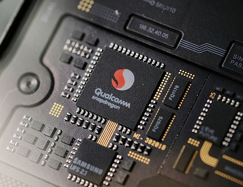
Phước Sang/unsplash.com
Qualcomm's next flagship mobile chip is now the most documented pre-announcement processor in Snapdragon history. Notebookcheck.net published an exclusive investigation on July 26 that combined a calibrated physical die measurement, a leaked internal graphics document, and a wave of previously unpublished modem and connectivity details to produce the most complete technical picture yet of the SM8975 — expected to debut as the Snapdragon 8 Elite Gen 6 Pro at Qualcomm's Snapdragon Summit in Maui, Hawaii, from September 22 to 24, 2026. For buyers weighing a premium Android phone in late 2026 or early 2027, the specs confirm one unavoidable takeaway: this chip will cost meaningfully more to put in a phone, and that cost will reach you at checkout.
The practical stakes are clear. Counterpoint Research has estimated that the combination of advanced chip costs and surging memory prices could push premium Android retail prices up by $150 to $200 per device. That figure matters because it tells you whether to buy now — at current Galaxy S26 Ultra or Xiaomi 17 Ultra prices — or to wait for a generation that will cost more but deliver capabilities that current hardware cannot match. The answer depends on which of those capabilities you actually care about.
Here is what the SM8975 brings, what it will cost, and what it cannot yet do.
Die and Process: Bigger Silicon on a Smaller Node
Notebookcheck's team calibrated the SM8975's physical die against Qualcomm's official package dimensions of 21.2 mm × 14 mm (0.835 in × 0.551 in) and arrived at a die measurement of approximately 12.6 mm × 10.67 mm (0.496 in × 0.420 in), or roughly 134 square millimeters. That is larger than the Snapdragon 8 Elite Gen 5's confirmed die area of 126.2 mm², even though the SM8975 moves to a more advanced manufacturing process.
The explanation is architectural complexity. The additional Matrix ALU blocks, a larger last-level cache, and a revised GPU take up area that the process-node shrink alone cannot recover. The SM8975 reportedly uses TSMC's N2P process — an enhanced 2nm-class node that employs nanosheet (gate-all-around) transistors, one step beyond the 3nm FinFET process used in the Snapdragon 8 Elite Gen 5. N2P's wafer cost has been modeled at roughly $33,000 per wafer, compared to approximately $20,000 for a 3nm wafer — a driver of the higher OEM pricing.
Running those inputs through a wafer-yield model using SemiAnalysis's Die Yield Calculator, Notebookcheck estimated a raw silicon cost of roughly $84 per good die before packaging, testing, binning, or IP licensing. That figure is a directional model, not a confirmed bill-of-materials number — TSMC does not publish N2P wafer pricing or defect-density data. The full platform cost OEMs actually pay bundles the SoC with RF transceivers and a FastConnect wireless chip, which inflates the real purchase price well beyond the raw die cost.
For competitive context, the SM8975 at 134 mm² remains smaller than MediaTek's Dimensity 9500 at approximately 140 mm², suggesting that Qualcomm's 2nm move is delivering real density gains even with the added compute blocks. The Apple A20 Pro, which is expected to power iPhone 18 Pro models later this year, uses the baseline N2 node rather than the enhanced N2P variant — meaning the SM8975 sits on a slightly more advanced process flavor than its Apple rival.
CPU: Third-Generation Oryon in a Familiar Layout
The SM8975 continues with a 2+3+3 Oryon core configuration — two prime cores, three performance cores, and three efficiency cores. That is the same core count as the standard SM8950 variant, which means Qualcomm's Pro-versus-standard split centers on GPU, memory, and connectivity, not raw CPU core topology. Qualcomm has not finalized clock speeds in any documentation Notebookcheck reviewed; circulating claims of peak speeds approaching 4.8 to 5.0 GHz should be treated as speculative until Qualcomm confirms them.
GPU: Adreno 850 vs. Adreno 845 — and the Feature That Divides Them
The SM8975 pairs with the Adreno 850, stepping up from the Adreno 840 in the outgoing Snapdragon 8 Elite Gen 5. Graphics memory (GMEM) holds at 18 MB rather than expanding, matching the prior generation rather than increasing. The gain over the Gen 5 is primarily in the driver stack — a more granular dynamic clock-and-voltage scaling implementation with better jank detection and improved responsiveness across simultaneous GPU contexts — and in the addition of two dedicated compute blocks that the standard SM8950 does not have.
The standard SM8950 uses a scaled-down Adreno 845 with 12 MB of GMEM, a 33 percent reduction that matters most in sustained GPU-intensive workloads where on-chip memory avoids bandwidth-hungry round-trips to system RAM.
AI Frame Fusion: Why Putting Matrix Compute Inside the GPU Matters
The headline GPU addition is AI Frame Fusion, enabled by two Matrix ALU blocks embedded in the Adreno 850's shader processor. These are purpose-built compute units designed to accelerate GEMM (general matrix multiply) and convolution operations — the mathematical core of nearly all neural network inference. The key architectural detail is not simply that matrix compute exists on the chip; Qualcomm's Hexagon NPU has included AI acceleration for generations. What is new is where these Matrix ALUs are placed: inside the GPU's shader processor, co-located with the GPU's GMEM pool.
That placement matters for frame generation specifically. A standalone NPU and the GPU occupy separate memory domains; running AI inference on an NPU while the GPU renders means data must travel across the chip's main interconnect bus. By placing the Matrix ALUs inside the shader processor, the SM8975 keeps the AI inference needed for upscaling and frame generation inside the same fast GMEM that the GPU is already using for rendering — eliminating the latency of that external bus trip. That is what makes real-time frame generation on a mobile phone GPU feasible in a way that NPU-to-GPU coordination would make much harder.
AI Frame Fusion operates in two modes, both exclusive to the Adreno 850 in the SM8975. The super-resolution mode takes motion vectors, a depth buffer, a low-resolution color buffer, and the previously rendered frame and reconstructs an upscaled output at 1080p or 1440p. The frame-generation mode uses motion-vector and optical-flow reprojection across the current and previous frames to synthesize an entirely new intermediate frame — effectively doubling perceived frame rates without proportionally increasing GPU power draw. The Adreno 845 in the standard SM8950 reportedly lacks both the Matrix ALUs and AI Frame Fusion, making this one of the sharpest hardware divides between the two chips.
The competitive landscape here is notable. NVIDIA's DLSS (Deep Learning Super Sampling) and AMD's FSR (FidelityFX Super Resolution) have demonstrated that AI-driven upscaling can deliver console-class visual quality at manageable power costs. AI Frame Fusion is Qualcomm's mobile-specific implementation of the same principle — and one that games would need to explicitly support to use, just as DLSS requires developer integration.
LPDDR6: Android Gets a Memory First
One of the SM8975's most consequential specifications is memory support. The chip will mark the first appearance of LPDDR6 RAM on an Android platform. OEMs may configure the SM8975 with either quad-channel 24-bit LPDDR6 or quad-channel 16-bit LPDDR5X, paired with 8 MB of last-level cache. The standard SM8950 is limited to LPDDR5X only.
LPDDR6 was standardized by JEDEC as JESD209-6 in July 2025 and uses a dual-subchannel architecture with 12 data lines per subchannel. Peak data rates reach up to 14.4 Gbps per pin, compared to 10.67 Gbps for LPDDR5X — a bandwidth improvement of roughly 35 percent at the high end. Samsung demonstrated working LPDDR6 silicon at CES 2026, reporting approximately 21 percent better power efficiency than the previous generation. Apple is reportedly sticking with LPDDR5X for the iPhone 18 series, leaving Android as LPDDR6's first mobile testing ground.
The AI angle is significant. Large language models running locally on a phone are increasingly limited by memory bandwidth, not by compute alone. A model that fits in RAM but cannot stream weights to the processor fast enough stalls inference in ways the user notices as sluggish response time. LPDDR6's bandwidth increase translates directly to faster on-device AI responses and higher-quality real-time image generation.
The cost problem is equally real. LPDDR6 currently carries a roughly 20 percent cost premium over LPDDR5X. Combined with the DRAM and NAND supply crisis that has already pushed memory component costs up 40 to 50 percent quarter-over-quarter in late 2025, that premium lands on top of an already elevated baseline. Counterpoint Research has stated directly that "higher retail prices are unavoidable in 2026 as rising costs will be passed to consumers," with the firm estimating a $150 to $200 increase per premium device. OEMs that choose LPDDR5X configurations to keep costs down will sacrifice the bandwidth advantage — and consequently some of the AI Frame Fusion pipeline performance.
Storage steps up to UFS 5.0 on the Pro, with two high-bandwidth lanes, versus UFS 4.0 or UFS 5.0 (single lane) on the standard variant depending on OEM configuration.
Modem and RF: Symmetric Upload Arrives for the First Time
The SM8975 pairs with Qualcomm's new X105 modem, its first appearance on a shipping Snapdragon platform. Both the SM8975 and the standard SM8950 reportedly use the same RF front end, which is not backward-compatible with prior-generation modems — meaning the standard Gen 6 will ship with some configuration of the X105 as well, rather than reusing prior-generation silicon.
The more technically significant RF story is the SDR885 transceiver. It is, per the leaked documentation Notebookcheck reviewed, Qualcomm's first sub-6 GHz transceiver to support 4×4 MIMO on both uplink and downlink simultaneously. In prior generations, uplink MIMO was limited — 2×2 uplink against 4×4 downlink was typical — meaning upload throughput was structurally capped below download speeds regardless of network conditions. The SDR885 removes that asymmetry with a 20-transmit-port configuration (arranged 7+7+3+3) and 16 primary plus 16 diversity receive-input paths, under 3GPP Release 18.
The SDR765, the sub-6 GHz-only companion transceiver, moves manufacturing from Samsung's 14nm RF process to TSMC's N6RF node — the same RF node used in Apple's C1 modem-RF system. It supports 2×2 MIMO uplink and 4×4 downlink, 1024-QAM modulation, and the n253, n255, and n256 satellite bands.
How Does Wi-Fi 8 Actually Work?
Both wireless companion chips — the WCN8841 and WCN8851, part of the FastConnect 8800 family — support Wi-Fi 8 in a 2×2 MIMO configuration at 300 MHz. Wi-Fi 8 is based on the IEEE 802.11bn amendment, which targets Ultra High Reliability (UHR) rather than simply higher peak throughput: the standard specifies at least a 25 percent reduction in 95th-percentile latency, a 25 percent improvement in throughput under real-world range conditions, and a 25 percent reduction in packet loss during access-point transitions. That means Wi-Fi 8 is designed to make wireless connections behave more like wired ones in congested environments — an advantage for cloud gaming, XR applications, and real-time video collaboration.
One important caveat: the 802.11bn standard has not yet been ratified and is not expected to reach final ratification until approximately 2028. Devices shipping in 2026 and early 2027, including those based on the FastConnect 8800, will operate on draft specifications. If the ratified standard diverges from the draft in ways that affect core operating parameters, early adopters could face compatibility limitations with certified Wi-Fi 8 access points. That scenario has precedent — Wi-Fi 6E and Wi-Fi 7 both saw interoperability issues in early deployments.
The two FastConnect chips differ by tier. The WCN8841 supports Bluetooth 6.0 and 2×2 MIMO at 300 MHz. The WCN8851 steps up with Bluetooth 7.0, a second Wi-Fi radio path capable of 2×4 or 4×4 MIMO at 320 MHz, Bluetooth 7.0 extended to the 5 GHz and 6 GHz bands, and ultra-wideband (UWB) for precision spatial positioning.
Which Phones Will Carry the SM8975 — and When?
Qualcomm's Snapdragon Summit 2026 is officially confirmed for September 22 to 24 in Maui, Hawaii. That is where the SM8975 is expected to be formally unveiled. Xiaomi is widely expected to be among the first out of the gate, potentially announcing a Gen 6 Pro-powered device alongside Qualcomm's keynote.
The SM8975 is expected to be reserved for a narrower tier of devices than the standard SM8950 — Ultra-branded phones, select foldables, and a small number of premium gaming devices. The Samsung Galaxy S27 Ultra is among the most-cited candidates, along with the Xiaomi 18 Ultra, Oppo Find X10 Ultra, and OnePlus 16. Most commercial handsets using the Gen 6 Pro are expected to appear in the second half of 2026 and through early 2027.
Qualcomm is reportedly offering a binned SM8975 variant — with lower CPU and GPU clock ceilings — at a reduced price to partners who want the silicon tier without paying for maximum clocks, mirroring the approach Apple uses with its A-series Pro and standard die differentiations. Some manufacturers may also trim camera hardware to offset SM8975's higher cost. Counterpoint Research has noted that LPDDR6 plus UFS 5.0 memory configuration costs can exceed the SoC cost itself at current memory prices — a Bill of Materials configuration that did not exist at this price tier in any prior Snapdragon generation.
Spec Breakdown: Gen 6 Pro vs. Gen 6
| Feature | Snapdragon 8 Elite Gen 6 Pro (SM8975) | Snapdragon 8 Elite Gen 6 (SM8950) |
|---|---|---|
| Process | TSMC N2P (2nm-class, enhanced) | TSMC N2 (2nm-class, baseline) |
| Die Size | ~134 mm² (~0.208 in²) | Not confirmed |
| CPU | 2+3+3 Oryon | 2+3+3 Oryon |
| GPU | Adreno 850, 18 MB GMEM | Adreno 845, 12 MB GMEM |
| Matrix ALUs | Yes (two blocks, shader-integrated) | No |
| AI Frame Fusion | Yes | No |
| RAM | LPDDR6 or LPDDR5X (OEM choice) | LPDDR5X only |
| Storage | UFS 5.0 | UFS 4.0 or UFS 5.0 (single lane) |
| L2 Cache (shared) | 16 MB | 16 MB |
| Last-Level Cache | 8 MB | 6 MB |
| Modem | X105 (full config) | X105 (reduced config) |
| Wi-Fi | Wi-Fi 8, FastConnect 8800 | Wi-Fi 8, FastConnect 8800 |
| Bluetooth | Up to 7.0 (WCN8851) | Up to 7.0 (WCN8851) |
| UWB | Yes (WCN8851 config) | Yes (WCN8851 config) |
| Expected launch | Snapdragon Summit, Sept. 22–24, 2026 | Snapdragon Summit, Sept. 22–24, 2026 |
All specifications are pre-announcement leaks; Qualcomm has not confirmed any SM8975 details.
Read more: Qualcomm's Snapdragon 8 Elite Gen 6 Pro Could Push Android Flagship Prices Even Higher
Should You Wait for a Gen 6 Pro Phone?
The decision splits cleanly along use case lines. If you are a high-fps mobile gamer, the combination of AI Frame Fusion and LPDDR6 bandwidth represents a genuine generational shift — better sustained frame rates, AI-assisted upscaling, and the memory bandwidth to run on-device AI models without cloud offload. If you primarily use your phone for productivity, photography, and communication, the standard Gen 6 or even a current Snapdragon 8 Elite Gen 5 device will cover most of your needs at a meaningfully lower price.
The timing risk cuts both ways. Buying now means avoiding the projected $150 to $200 price increase and getting a device that is not contingent on unconfirmed specifications. Waiting means access to the first Wi-Fi 8 and LPDDR6 Android phones — but also exposure to potentially higher prices, potential Wi-Fi 8 compatibility growing pains, and the likelihood that early Gen 6 Pro supply will be constrained to a small set of Ultra-tier launches.
Read more: Samsung's Galaxy S27 May Add a "Pro," Its First Four-Model Flagship Lineup
Frequently Asked Questions
When will the Snapdragon 8 Elite Gen 6 Pro be officially announced?
Qualcomm has confirmed Snapdragon Summit 2026 for September 22 to 24 in Maui, Hawaii. That is the expected venue for the chip's official unveiling. Commercial devices based on the SM8975 are expected to follow in the second half of 2026 and into early 2027, with Xiaomi widely anticipated as one of the first OEM partners to announce a Gen 6 Pro handset.
What exactly is AI Frame Fusion, and how is it different from what current Android phones can do?
AI Frame Fusion uses two Matrix ALU blocks embedded inside the Adreno 850's shader processor — the same computing blocks that handle rendering — to run neural network inference on a game's motion and depth data. The super-resolution mode reconstructs high-resolution frames from lower-resolution rendering output; the frame-generation mode synthesizes new frames between rendered frames to increase perceived frame rate. Current Android flagships rely on the Snapdragon Game Super Resolution (SGSR) system, which uses fixed-function rather than Matrix ALU-accelerated upscaling and does not include frame interpolation. No Android phone currently supports GPU-shader-integrated AI frame generation.
Will the Snapdragon 8 Elite Gen 6 Pro make my next Ultra phone significantly more expensive?
Almost certainly yes, if you choose LPDDR6 memory. Counterpoint Research has estimated that the combination of advanced chipset costs and the ongoing DRAM/NAND supply crisis will push premium Android retail prices up by $150 to $200. LPDDR6 itself carries a roughly 20 percent cost premium over LPDDR5X. The SM8975 does allow OEMs to use LPDDR5X instead, which would reduce the memory cost component — but that choice also sacrifices the bandwidth advantage that makes LPDDR6 meaningful for AI workloads. Expect to see the full price impact most clearly in Galaxy S27 Ultra and Xiaomi 18 Ultra pricing.
What does symmetric 4×4 MIMO uplink mean for everyday connectivity?
In prior Snapdragon generations, the modem supported 4×4 MIMO for downloads but typically only 2×2 MIMO for uploads, meaning upload speeds were structurally slower than download speeds regardless of the network. The SDR885 transceiver in the SM8975 generation introduces 4×4 MIMO on both uplink and downlink — the first time this configuration has appeared in a Snapdragon platform. In practical terms, this means the theoretical ceiling for mobile upload speeds will be meaningfully higher on Gen 6 Pro devices, which matters for large file uploads, real-time video streaming, and cloud-sync-heavy workflows on 5G networks.

-
 C114 Communication Network
 -
 Communication Home
