
 Search

Tsmc.com
Taiwan Semiconductor Manufacturing Company added $100 billion to its Arizona commitment Thursday, raising its total US pledge to $265 billion across 12 facilities — the largest direct investment from a foreign company in American history — as the world's biggest contract chipmaker posted its fifth consecutive record quarterly profit.
The expansion is not just more factory floor space. TSMC's announcement adds dedicated advanced packaging capacity to Arizona — specifically, CoWoS (Chip on Wafer on Substrate), the 2.5D packaging technology that every major AI accelerator on the market depends on to ship as a functional product. CoWoS capacity, not silicon wafer production, is the single binding constraint currently controlling how many AI accelerators NVIDIA, AMD, and the major cloud hyperscalers can deliver to buyers. The Arizona CoWoS expansion announced Thursday directly targets that constraint.
Despite the record results, TSMC's US-listed shares fell more than 2% on the day. A JPMorgan equity trader attributed the selloff to inflated expectations rather than negative news, saying investor sentiment reflects how elevated the bar has gotten for the semiconductor sector given the prior months of outperformance driven by AI excitement.
Read more: TSMC Posts Record Quarter as AI Chip Demand Pushes Full-Year Growth Outlook Past 40%
Record Earnings Drive a Quarter-Trillion-Dollar Commitment
TSMC Chairman and CEO C.C. Wei disclosed the additional $100 billion commitment at the company's Q2 2026 earnings conference in Taipei, where he also reported net income of NT$706.56 billion ($22 billion), a 77.4% increase year-over-year. Revenue reached NT$1.27 trillion ($40.2 billion), up 36% from a year earlier and ahead of Wall Street consensus — analysts had expected NT$1.264 trillion in revenue and NT$632.64 billion in net income.
Gross margin for the quarter reached 67.7%, up 1.5 percentage points sequentially, driven by cost improvements and higher utilization across leading-edge nodes. Chips made on 7-nanometer or smaller process nodes represented 77% of total wafer revenue. The 5nm node led with a 33% share, with 3nm close behind at 30%. High-performance computing — the category that includes AI accelerators — accounted for 66% of quarterly revenue, up 20 percentage points from the previous quarter.
CFO Wendell Huang attributed the performance to relentless demand for leading-edge process technologies, with a steep ramp-up of 2-nanometer production already underway. For Q3 2026, TSMC guided revenue of $44.6 billion to $45.8 billion, with an operating profit margin of 56% to 58%. For full-year 2026, the company now expects revenue growth slightly above 40% in US dollar terms, up from previous guidance of more than 30%.
Capital expenditure guidance for 2026 was also revised sharply upward, to $60 billion to $64 billion from a prior range of $52 billion to $56 billion. About 70% to 80% of that budget is earmarked for advanced process technologies.
Analysts at Goldman Sachs had already flagged that TSMC's production capacity would likely continue to lag surging AI demand near-term — making the capex increase expected, if not welcomed by short-term holders.
CoWoS Expansion Addresses AI's Binding Constraint
Understanding why the packaging facilities announced Thursday matter requires a brief technical detour.
CoWoS — Chip on Wafer on Substrate — is TSMC's 2.5D advanced packaging architecture. It solves a problem that raw silicon manufacturing cannot: connecting a high-performance logic die (a GPU or a custom AI accelerator) to multiple stacks of High Bandwidth Memory (HBM) at extremely high data transfer rates while keeping power and latency under control. The interposer at the center of a CoWoS package contains high-density metal interconnects and through-silicon vias (TSVs), enabling chip-to-chip data paths that are physically impossible to replicate on a printed circuit board. Every NVIDIA H100, H200, B100, B200, and GB200 ships on CoWoS, as does every AMD MI300 and MI400. Without it, a fabricated AI accelerator die is not a shippable product.
TSMC has roughly doubled CoWoS capacity annually since 2023, yet demand continues to outpace supply. At its May 2026 North America Technology Symposium, TSMC projected an eleven-fold increase in AI accelerator wafer shipments between 2022 and 2026. Industry analyses indicate CoWoS substrate supply — specifically the ABF (Ajinomoto Build-up Film) needed for redistribution layers — remains the primary bottleneck for AI chip delivery timelines through at least late 2027, even after TSMC's current expansion efforts.
The Arizona CoWoS expansion changes the geographic distribution of that bottleneck, adding capacity on US soil and giving hyperscalers with domestic-sourcing requirements a path to AI accelerators that does not route entirely through Taiwan.
Read more: TSMC Q2 Earnings July 16: Three CoWoS Signals That Test AI's Spending Ceiling
What Is Already Built — and What Is Coming
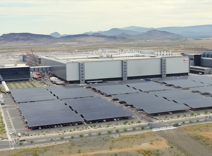
TSMC's North Phoenix campus is not a future promise. Fab 21 Phase 1 entered volume production of 4nm chips in Q4 2024, supplying Apple, NVIDIA, and other leading customers. Arizona production revenue is expected to grow from roughly 2% of TSMC's total revenue in 2025 to 4% to 5% by 2027. The facility reported a profit of NT$16.14 billion ($514 million) in its first full year of mass production in 2025, according to Taiwan's National Development Council head Yeh Chun-hsien. Apple purchased more than 100 million chips manufactured at the Arizona campus in 2026.
Yield performance at the Arizona fab has exceeded skeptics' expectations. Fab 21 Phase 1 has reached approximately 92% yield on 4nm production — by one report, slightly above yields at comparable TSMC facilities in Taiwan. That figure matters because replicating Taiwan's manufacturing discipline in a greenfield US location was the central argument against the CHIPS Act investment thesis.
The second fab — Fab 21 Phase 2, targeting 3nm and eventually 2nm production — completed construction in April 2026. Equipment installation began in Q3 2026, with volume production now targeted for 2027, roughly a year ahead of the original 2028 schedule. A third fab, targeting 2nm and the A16 process node, broke ground in April 2025 and is expected to reach production by the end of the decade.
The four additional fabs announced Thursday will target 2-nanometer and below process technologies, alongside the CoWoS packaging capacity. Wei said TSMC will "probably" build four more fabs in Arizona, without committing to a specific construction timeline.
Upon completion of all announced facilities, approximately 30% of TSMC's 2nm and more advanced global capacity will be located in Arizona.
From FinFET to Gate-All-Around: Why the Node Progression Matters
The node sequence being built in Arizona represents more than incremental improvement. Semiconductor fabrication process nodes — labeled in nanometers — have been marketing terms rather than literal physical measurements for decades. What the numbers do track is generational capability.
The 4nm node currently in production at Fab 21 Phase 1 uses FinFET transistor architecture — the design that has dominated since the 22nm generation. The 3nm node also uses FinFET, with a 15% speed improvement at the same power draw, or a 30% reduction in power at equivalent speed.
The 2nm node marks a structural architectural transition: from FinFET to Gate-All-Around (GAA) nanosheet transistors. GAA wraps the transistor gate around the channel on all four sides rather than three, improving electrostatic control and reducing current leakage as transistors shrink toward near-atomic scales. Volume 2nm production began in Taiwan in late 2025 at TSMC's Fab 22 in Kaohsiung, where 2nm wafers now cost more than $30,000 — nearly double the 4nm wafer price — reflecting both technical complexity and constrained supply.
Beyond 2nm, the A16 (1.6nm-class) node introduces backside power delivery — routing power wiring through the back of the silicon wafer rather than the front. This frees the front surface for signal routing and enables higher transistor density than front-side power delivery allows. A16 is among the nodes targeted at Arizona's facilities, making the campus a planned home for the most architecturally advanced production processes in commercial semiconductor manufacturing.
Barclays senior semiconductor analyst Daniel Morgan described the 2nm transition as "not incremental — it's transformational," adding that power efficiency gains alone could enable a 30% increase in AI training throughput per rack, which "fundamentally changes the economics of data center investment."
Trade Deal Architecture Behind the Investment
The January 15, 2026 US-Taiwan trade and investment agreement, negotiated through the American Institute in Taiwan and the Taipei Economic and Cultural Representative Office, established the framework that structured this investment. Under the agreement, Taiwanese semiconductor and technology enterprises committed a minimum of $250 billion in direct investment in US semiconductor, energy, and AI production capacity, while Taiwan pledged an additional $250 billion in credit guarantees to support further expansion. In return, the US reduced reciprocal tariffs on Taiwanese goods to 15%, down from 20%.
Commerce Secretary Howard Lutnick credited the administration's trade posture directly: "President Trump's leadership is driving companies to invest in American manufacturing. TSMC's announcement of an additional $100 billion investment following our historic deal on trade and investment with Taiwan will create tens of thousands of American jobs and bring advanced semiconductor manufacturing back to America."
Wei echoed the framing from Taipei: "We appreciate the strong collaboration and support of the Trump Administration, Secretary Lutnick and our leading US customers," he said.
Arizona Governor Katie Hobbs described the campus as "the nation's epicenter for advanced semiconductor manufacturing and innovation," noting that Arizona has attracted more than 70 semiconductor-related expansions since 2020, representing over $314 billion in total investment across the full supply chain. Phoenix Mayor Kate Gallego called it "the largest deal in US history."
The CHIPS and Science Act of 2022 catalyzed the initial US push. TSMC's Arizona project received a finalized grant of up to $6.6 billion in direct funding from the Commerce Department's CHIPS Program Office in November 2024. That award covered the first three fabs. The terms governing the new tranche have not yet been disclosed.
Execution Risks Are Real and Officially Acknowledged
Wei was careful not to commit to a construction schedule, saying Thursday that the speed of expansion would track customer demand. That qualification reflects documented operational constraints the campus continues to navigate.
As recently as May 2026, Taiwan's National Development Council head Yeh Chun-hsien — following an inspection visit to the Arizona hub — identified four primary hurdles: utilities constraints (particularly water supply in Arizona's desert environment), regulatory complexity, visa processing delays, and labor shortages. More than 1,000 Taiwanese engineers sent to Arizona on three-year assignments are now approaching the end of their contracts, raising continuity questions about the specialized workforce that built the fab's yield performance.
Water use is a legitimate constraint but not a crisis. Three TSMC fabs are estimated to use approximately six billion gallons annually, with reclamation rates of 65% to 90% — representing about 0.26% of Arizona's statewide annual water use of 2.3 trillion gallons.
The semiconductor industry faces an estimated shortage of one million workers globally by 2030, and replicating the institutional knowledge behind Taiwan's manufacturing precision remains the longest-term operational challenge for the Arizona campus.
ASML, TSMC's primary supplier for the extreme ultraviolet (EUV) lithography tools required for leading-edge production, raised its own 2026 outlook on July 15 — the day before the TSMC announcement. Applied Materials CEO Gary Dickerson has publicly forecast years of capacity expansion ahead. The supplier ecosystem is moving in lockstep with the buildout.
What Does This Mean for the Geopolitical Supply Chain?
Taiwan produces more than 90% of the world's most advanced semiconductors, a geographic concentration that defense planners and supply chain executives have described as a structural vulnerability. A disruption in Taiwan from weather, infrastructure failure, or geopolitical escalation would slow AI accelerator delivery globally with no short-term alternative.
Upon completion of the full Arizona commitment, 30% of TSMC's 2nm-and-below capacity will be in the US. That does not eliminate the Taiwan concentration, but it provides the first meaningful geographic hedge for the most advanced nodes in commercial production.
Wei also addressed concerns that the US expansion might hollow out domestic Taiwanese capacity, noting that TSMC is planning 13 leading-edge and advanced packaging fabs in Taiwan over the same period. Taiwan remains TSMC's primary manufacturing hub; Arizona is additive, not substitutive.
For investors and supply chain planners, the capex increase — to $60 billion to $64 billion in 2026 alone, up from a prior range of $52 billion to $56 billion — signals TSMC's management assessment that the AI demand cycle will sustain at least through 2029 to 2030 by Wei's own public estimate. For investors concerned about free cash flow compression during the spending cycle, Q2 free cash flow was NT$287.36 billion — substantial, but monitored closely against a capex bill that now exceeds what TSMC spent in the prior three years combined.
As Wei put it from the Taipei conference room where the commitment was made, he expressed confidence in the tremendous opportunities that lie ahead for the company.
Frequently Asked Questions
How does TSMC's Arizona investment affect AI chip availability?
The most immediately consequential part of the July 16 announcement is the addition of CoWoS advanced packaging facilities — not just wafer fabs. CoWoS is the 2.5D packaging technology that connects AI accelerator dies to High Bandwidth Memory and enables chips like NVIDIA's H100 and H200 to function as shippable products. CoWoS capacity — not raw silicon production — is currently the binding constraint on AI accelerator supply through at least late 2027. Adding CoWoS capacity in Arizona directly targets the bottleneck that is determining AI hardware delivery timelines for hyperscalers.
What is the difference between the 4nm, 2nm, and A16 chips being made in Arizona?
These are generational process nodes with distinct transistor architectures, not just incremental size reductions. The 4nm node (currently in production at Fab 21 Phase 1) and the 3nm node (Fab 21 Phase 2, targeting 2027 production) use FinFET transistor architecture. The 2nm node marks a structural shift to Gate-All-Around (GAA) nanosheet transistors, which wrap the gate around the channel on all four sides for better control at near-atomic transistor scales — enabling 10% to 15% speed improvements or 25% to 30% power reductions compared to 3nm. The A16 (1.6nm-class) node goes further, adding backside power delivery that routes power wiring through the back of the wafer, freeing the front for higher transistor density. Both 2nm and A16 production are planned for Arizona, which would make the Phoenix campus home to the most architecturally advanced commercial semiconductor processes ever produced in the United States.
When will TSMC Arizona be fully operational and producing the most advanced chips?
Fab 21 Phase 1 (4nm) is already in volume production and profitable. Phase 2 (3nm) began equipment installation in Q3 2026, with volume production now pulled forward to 2027 — about a year ahead of the original 2028 schedule. The third fab (2nm and A16), which broke ground in April 2025, is expected to reach production by the end of the decade. The four additional fabs announced July 16 do not yet have committed construction timelines; Wei said expansion pace will track customer demand. Full build-out of all 12 facilities — 10 wafer fabs, two advanced packaging facilities, and an R&D center — is a project that extends well into the 2030s.
What are the main risks that could slow or derail the Arizona expansion?
The four constraints TSMC itself has officially identified are: water supply in Arizona's desert environment, regulatory complexity, visa processing delays for specialized overseas engineers, and general labor shortages in a region without deep semiconductor manufacturing heritage. More than 1,000 Taiwanese engineers on three-year assignments are approaching contract expiration, creating a near-term workforce continuity question. Construction timelines for the four new fabs depend on whether AI-driven customer demand remains robust enough to justify the capital outlay — the same dynamic that caused TSMC's stock to decline even on a record earnings day, as investors weighed whether accelerating capex would compress free cash flow.

-
 C114 Communication Network
 -
 Communication Home
