
 Search

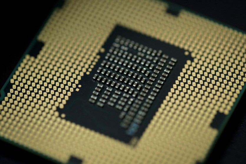
A computer processor is pictured on January 5, 2018 in Paris. Thomas SAMSON/gettyimages.com
A photomask standard that has governed semiconductor manufacturing since the 1980s is on its way out. On September 7 and 8, 2026, Taiwan Semiconductor Manufacturing Company and Dutch lithography giant ASML announced a joint initiative to transition the chipmaking industry from its 40-year-old 6-inch photomask standard to a new 12-inch format — and four of the world's most consequential chipmakers simultaneously committed to the direction, all timed to the SPIE BACUS Photomask Technology conference in Monterey, California. Samsung Electronics confirmed it would join the initiative; Intel Foundry separately disclosed that it had been leading a parallel large-format mask effort for more than three years. The initiative — formally called a Large Mask Consortium — targets a 12-inch mask pilot line by 2031 and full High-NA lithography system readiness for advanced-node production by 2033.
The four companies did not converge on this moment out of commercial enthusiasm. They converged out of physics.
What a Photomask Is, and Why Bigger Matters for AI Chips
A photomask — also called a reticle — is the precision stencil through which a lithography machine shines light to transfer circuit patterns onto a silicon wafer. Think of it as an extremely precise template: the chip's circuit layout is etched into the mask, and the scanner projects that pattern at reduced scale onto the wafer below, layer by layer, until a complete chip emerges.
For decades, the industry has used 6-inch square masks. That standard worked well because conventional EUV and older DUV scanners demagnify the mask pattern symmetrically in both directions — a 4× reduction horizontally and 4× vertically — producing an exposure field roughly 26 mm × 33 mm (1.02 in × 1.30 in) on the wafer, large enough to accommodate most chip die sizes.
High-NA EUV, however, changed the equation in a way that no software update can fix. ASML's High-NA systems — sold as the EXE series — increase numerical aperture from 0.33 to 0.55, enabling the resolution needed to print features at 2-nanometer nodes and beyond. But achieving that higher resolution required ASML's engineers to adopt an anamorphic optical design: a system that demagnifies the mask pattern differently in the horizontal and vertical directions. The result is 4× demagnification horizontally and 8× demagnification vertically.
This asymmetry is not an engineering oversight. It is a physical consequence of increasing the numerical aperture. At higher NA, the optical beam occupies more angular extent; to prevent the incoming illumination beam and the reflected beam from overlapping at the mask surface, the magnification must be made asymmetric. The anamorphic design solves that problem — and creates a new one. Because the scanning-direction demagnification doubled (from 4× to 8×), the same 6-inch mask now projects onto half the prior wafer coverage in that direction. The exposure field shrinks from 26 mm × 33 mm to 26 mm × 16.5 mm (1.02 in × 0.65 in) — roughly half the area of a conventional EUV shot.
There is no setting to turn up, no firmware to update, and no clever patterning algorithm that restores the field. The reduced field is a law of optics.
The Stitching Problem: A 30% Tax on the World's Most Expensive Machines
For small chip dies — smartphone processors, some memory devices — the reduced 26 × 16.5 mm field is workable. For the large dies that AI accelerators require — and that are increasingly central to the semiconductor industry's business — it is not.
When a die is too large for a single High-NA EUV exposure, chipmakers must split the die into two overlapping half-fields, expose the wafer twice, and then align the two exposures at a seam to sub-nanometer tolerances. This technique is called reticle stitching.
Stitching works, but it exacts a steep price. According to data that Intel presented at the SPIE conference, stitching reduces High-NA scanner wafer output from approximately 175 wafers per hour to around 125 — a productivity loss of nearly 30%. That matters because each ASML EXE series High-NA EUV scanner costs approximately $380 million to $400 million per unit — roughly double the cost of a standard EUV tool — and Samsung's September 8 announcement disclosed the won-denominated figure at approximately 500 billion Korean won (approximately $372 million at the September 8, 2026 mid-market rate of 1,343 won per dollar), consistent with other published figures. When a tool in that cost range runs at 70% of its design throughput, every chip it produces carries a higher embedded capital cost — and that cost ultimately flows through to the economics of AI infrastructure.
Beyond throughput, stitching forces chip designers to build the seam boundary into their floor plans from the outset, constraining layout options for dense, high-performance designs. Any misalignment at the seam risks yield loss at exactly the location where die performance is most sensitive. As analysis of the initiative has noted, stitching adds design rules, alignment requirements, process complexity, and potential yield risk at the seam — making it a structural tax on every layer that requires High-NA exposure.
The 12-inch mask — specifically the 6-inch × 12-inch rectangular format — resolves the geometry by doubling the mask's length in the scanning direction. Because the scanning-direction demagnification is 8×, a 12-inch mask in that dimension corresponds to the same 33 mm wafer-side coverage that a 6-inch mask achieved under the old symmetric 4× system. The full 26 mm × 33 mm exposure field is restored. Large dies, including AI accelerators, can be printed in a single shot. The 30% throughput penalty disappears.
Read more: Intel Leads Foundry Race With First High-NA EUV Logic Chip in Mass Production
The Consortium: What Was Announced and by Whom
The joint TSMC–ASML initiative was established on September 7, ahead of the SPIE BACUS conference, and announced publicly on September 8.
ASML CEO Christophe Fouquet described the timeline as progressive. "We expect the adoption of High NA EUV to increase progressively along the device scaling roadmap, first using current 6-inch masks and then further supported by 12-inch masks, which enable greater scanner productivity and allow the industry to meet the demand for smaller, faster and more energy-efficient chips," Fouquet said.
TSMC Chairman and CEO Dr. C.C. Wei framed the effort as an exercise in ecosystem collaboration that no single company could drive alone. "We have always believed that when the industry works together to solve complex problems, we unlock possibilities that no single company could achieve alone," Wei said. "By bringing together expertise from across the industry's value chain, we hope to keep providing the benefits of cutting-edge technology through continuous innovation that lowers barriers and puts advanced solutions accessible at scale."
TSMC has committed to deploying High-NA EUV in high-volume manufacturing for advanced nodes starting in 2030, with the number of layers requiring the technology expected to grow as transistor architectures advance — driven primarily by AI application complexity.
Samsung confirmed it would join the consortium and contribute both memory and foundry manufacturing experience. The South Korean company announced a separate enhanced strategic partnership with ASML the same day, and set a more aggressive near-term timeline: it plans to become the first chipmaker in the industry to apply High-NA EUV to high-volume DRAM manufacturing by 2028 — ahead of any 12-inch mask availability, using current 6-inch format with stitching in the interim. Samsung CEO Jun Young-hyun said the AI era is increasing the importance of technological innovation across the semiconductor value chain. SK Hynix is separately evaluating its own participation in the consortium.
Intel's position is distinct from its partners'. The company has already processed more than one million wafers using High-NA EUV lithography — not only in research and development but in volume production on select layers of its Core Ultra Series 3 Panther Lake processors, built on Intel's 18A process node. Intel also disclosed at the SPIE conference that it has led the 6×12-inch format effort for more than three years, working with ASML, mask makers, EDA partners, and materials suppliers to develop the foundational standards and infrastructure needed for the transition. The coordinated September 8 announcements from TSMC and Samsung effectively validated the direction Intel has been pursuing independently.
An Infrastructure Overhaul That Touches Everything Upstream
The scale of what the 12-inch transition will require should not be underestimated. Unlike a new chip process node — which primarily concerns the fab and its lithography equipment — a mask format change propagates backward through an entirely separate supply chain that is currently organized around the 6-inch square standard established decades ago.
Christopher Progler, a veteran photomask industry executive, described the scope in an earlier interview with Semiconductor Engineering: "If the industry adopts a 6 x 12-inch mask format, that's going to be a significant disruption. It affects everything, from the way you manufacture the mask substrate to the mask writers, etchers, and inspection tools. Basically, every tool involved in making masks would need to be redesigned or replaced to varying degrees. If that change happens, it's going to ripple through the entire supply chain."
That supply chain includes mask blank substrate suppliers (who must produce glass substrates with flatness tolerances appropriate for the new rectangular format), electron-beam pattern writers, pellicle manufacturers (whose films protect masks from particle contamination and must withstand higher EUV source power under High-NA conditions), defect inspection systems, overlay metrology equipment, and the robotic handling and storage infrastructure that moves masks through a fab. Every category requires engineering work specific to the new format. The 2031 pilot line target gives the ecosystem roughly five years to develop, qualify, and integrate those tools in parallel — a timeline that industry observers describe as ambitious given the scope of the upstream challenge.
Why This Matters Beyond the Fab
The chips that will eventually be manufactured using 12-inch High-NA EUV masks — logic devices at 2nm-class nodes and below — are the processors and AI accelerators that will underpin the next generation of computing infrastructure.
TSMC noted explicitly that growing AI application complexity is the primary driver behind the expected increase in High-NA EUV layers per device. As transistor architectures evolve to handle ever-larger AI models, the geometric precision that High-NA provides becomes not optional but necessary — and the productivity economics of running those expensive tools without stitching penalties become a meaningful factor in the cost of every chip those architectures require.
The 2033 production readiness date aligns with what industry roadmaps project as the volume ramp of process nodes below 2nm. If the initiative stays on schedule, chipmakers will arrive at that transition with an infrastructure capable of exploiting High-NA EUV's full potential — rather than working around its current field constraints — at the moment when AI chip demand for those nodes is expected to be at its highest.
Read more: ASML Raises Full-Year Guidance as Intel Ships First High-NA EUV Logic Chip
What Remains to Be Proven
For all the momentum of the September 8 announcements, the 12-inch photomask initiative is still a development program — not a completed transition.
Mask quality specifications for the new format will need to be established, tested, and qualified across every participating chipmaker's process stack. Those specifications include substrate flatness tolerances, defect density limits, pellicle durability under elevated EUV source power, and overlay performance across the full 33mm scanning direction. The Semiconductor Engineering interview with Progler underscores that these are not incremental refinements to existing standards; they are new requirements, and the tooling to meet them does not yet exist at production scale.
A shared infrastructure project also does not guarantee identical adoption schedules. Samsung's aggressive 2028 DRAM timeline, TSMC's measured 2030 high-volume approach, and Intel's existing production deployment reflect genuine differences in manufacturing priorities, process node strategies, and risk appetite. The consortium's value is alignment on a destination format, not a synchronized march.
What the coordinated announcements on September 8 accomplished is arguably more important than any single technical milestone: four of the world's most consequential semiconductor companies, plus the dominant lithography equipment supplier, formally aligned on a common infrastructure direction — and they did it in public, at a technical conference, within hours of each other. In an industry where infrastructure decisions can take a decade to fully play out, that alignment itself is the news. The physics determined what the destination would be. The consortium determines when the industry will get there together.
Frequently Asked Questions
What is a photomask, and why does its size matter for chipmaking?
A photomask (also called a reticle) is the master template that a lithography machine uses to project circuit patterns onto a silicon wafer. The scanner shines light through the mask pattern and focuses it at reduced scale onto a wafer coated in photosensitive material. The industry has used 6-inch square masks for decades. Size matters because ASML's High-NA EUV scanners use an asymmetric (anamorphic) optical design that shrinks the wafer-side exposure field to 26 mm × 16.5 mm (0.65 in) instead of the standard 26 mm × 33 mm (1.30 in). A 12-inch (6 in × 12 in) mask restores that full exposure field, removing the need to split large dies across two exposures.
Why can't chipmakers just use software to fix the reduced exposure field in High-NA EUV?
The field size reduction is not a software problem — it is a physical consequence of the laws of optics. Increasing the numerical aperture of an optical system increases its resolution, but the étendue (optical invariant) constrains how much imaging area the system can cover simultaneously. At 0.55 NA, ASML's EXE scanners must use anamorphic optics to split demagnification (4× horizontal, 8× vertical) to prevent the beam geometries from conflicting at the mask surface. That 8× vertical demagnification halves the wafer-side field. No firmware update, patterning algorithm, or design rule can restore a field that is physically limited by the optics. The only complete solution is a larger mask — which is exactly what the 12-inch format provides.
When will the 12-inch photomask transition actually affect chips that consumers or enterprises can buy?
The initiative's milestones are a 12-inch mask pilot line by 2031 and full High-NA lithography system readiness for advanced-node production by 2033. That timeline aligns with the volume ramp of chip nodes below 2nm. Chips benefiting from the full productivity of the 12-inch format — particularly large-die AI accelerators that currently require stitching — are likely a 2033-plus production story. In the interim (2026–2030), High-NA EUV will continue to use 6-inch masks with stitching where necessary. Samsung's more aggressive schedule — Samsung's High-NA DRAM timeline targets 2028 — will still use 6-inch masks in that initial phase.
What does the supply chain overhaul actually involve, and why does it take until 2031?
The 12-inch format change affects every piece of equipment in the photomask manufacturing supply chain — not just the lithography scanners that use the masks. Photomask blank suppliers must produce glass substrates with new flatness and purity specifications. Electron-beam mask writers — the tools that pattern the circuit design onto the mask blank — must be redesigned for the new rectangular format. Pellicle manufacturers must develop films that protect the larger mask surface while withstanding higher EUV source power. Defect inspection systems, overlay metrology tools, and robotic handling and storage equipment all require format-specific redesigns. Industry veteran Christopher Progler has described this as a disruption that means "every tool involved in making masks would need to be redesigned or replaced to varying degrees." The 2031 pilot line target gives this supply chain roughly five years to develop and qualify those tools before the 2033 production readiness milestone.

-
 C114 Communication Network
 -
 Communication Home
