
 Search

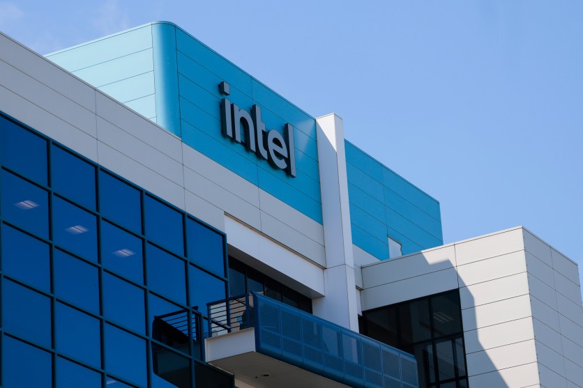
JULY 23: Intel headquarters is seen on July 23, 2026 in Santa Clara, California. Intel reported over $16 billion in sales for the second quarter of the year. Heather Diehl/GettyImages.com
Intel Foundry disclosed Monday at the SPIE Photomask Technology + Extreme Ultraviolet Lithography conference in Monterey, California, that it has now processed more than one million 300mm wafers using High Numerical Aperture (High-NA) Extreme Ultraviolet (EUV) lithography — a cumulative total that exceeds the output of every other chipmaker on earth combined. The joint Intel-ASML announcement, released on Monday morning, arrived one day after TSMC and ASML jointly unveiled a formal industry initiative to transition the semiconductor industry to 12-inch photomasks for High-NA EUV — validating a campaign Intel has led alone for more than three years and dramatically raising the odds that stitching, the workaround that defines today's High-NA production floor, has a concrete expiration date.
The scale of Intel's lead is worth stating plainly. In early 2026, ASML confirmed that all High-NA EUV systems it had shipped to all customers combined had processed more than 500,000 wafers while achieving above 80% availability — a benchmark that formally cleared the technology for production. Intel alone has now surpassed that figure by a factor of more than two. As recently as late February 2025, Intel engineers were running approximately 30,000 cumulative High-NA wafers on two EXE:5000 R&D systems; the company has since added at least one ASML Twinscan EXE:5200B production scanner and crossed the million-wafer mark in roughly 19 months. That is not a "first" announcement of the kind Intel and ASML made in July — it is proof that the technology has moved from laboratory curiosity to factory workhorse.
TSMC Joins the Initiative Intel Founded
The more consequential disclosure of the weekend may not be Intel's wafer count, but what happened Sunday. On September 7, in advance of the annual SPIE BACUS Conference in Monterey, ASML and TSMC established an industry-wide collaborative initiative to drive the transition to 12-inch photomasks for High-NA EUV. The initiative targets establishing a 12-inch mask pilot line by 2031, paving the way for full High-NA lithography system readiness for advanced-node production by 2033.
Read more: Intel Leads Foundry Race With First High-NA EUV Logic Chip in Mass Production
TSMC Chairman and CEO C.C. Wei stated in the joint press release that when the industry works together on complex problems, it unlocks possibilities no single company could achieve alone. Separately, ASML President and CEO Christophe Fouquet said in Monday's Intel/ASML announcement that Intel Foundry had been one of the key leaders of the industry's adoption of High-NA EUV, from installing the first commercial EXE system in 2024, to qualifying the latest generation of tools, to shipping the first high-volume logic product manufactured with High-NA EUV.
Intel has led an industry initiative for the larger 6×12-inch format for more than three years, working alongside ASML, mask makers, EDA partners, and materials providers to develop the standards and infrastructure needed for future High-NA scaling. For three of those years, Intel was largely the initiative's sole evangelist among volume logic producers. TSMC's formal entry into the initiative changes that calculation fundamentally: the world's dominant contract chipmaker has now publicly committed to the same destination Intel has been pointing toward, with a timeline that makes 2033 the earliest date at which the 12-inch standard could begin reshaping production economics.
TSMC officially intends to use ASML's High-NA technology in high-volume manufacturing for advanced nodes starting in 2030. As technology nodes advance, TSMC expects the number of layers requiring High-NA EUV to rise, driven primarily by the increasingly complex transistor architectures required for AI applications.
Why Stitching Is the Constraint That Makes 6×12 Matter
To understand why the photomask format debate carries stakes, it helps to understand what stitching costs.
Standard EUV lithography uses 4× magnification in both horizontal and vertical directions, enabling a 26×33mm (approximately 1.02×1.30 inches) exposure field on the wafer from a standard 6-inch (152mm) photomask. ASML's High-NA scanners, by contrast, use an anamorphic optical design with 4×/8× magnification — the same 6-inch mask now produces only a 26×16.5mm (1.02×0.65 inch) half-field on the wafer. For a chip die that is larger than 26×16.5mm, the die must be exposed in two separate half-field passes and the results aligned with sub-nanometer precision. That technique is called stitching, and it carries three distinct costs.
First, stitching significantly reduces throughput. On an ASML EXE:5200B, the production-grade High-NA scanner, throughput drops from 175 to 125 wafers per hour when stitching is required — a reduction of 50 wafers per hour, or roughly 29% of the tool's maximum capacity. For a technology platform that already carries a significantly higher per-exposure cost than conventional EUV, a 29% throughput penalty adds meaningfully to the per-chip cost of manufacturing on High-NA EUV.
Second, chip designs must be architected around stitching from the floor-planning stage, meaning the stitch boundary constrains where logic blocks, memory arrays, and interconnects can be placed. Intel Foundry has developed process design kit (PDK) solutions to help customers floor-plan within the existing 6-inch mask format, and ASML's Jan van Schoot is scheduled to present research on scanner and mask stitching requirements this afternoon at the SPIE conference. Intel Foundry's Kimberly Pierce is also scheduled to present "High NA EUV: stitching for manufacturing" in the same session. Both talks will address the engineering state of the near-term stitching path.
Third, any overlay misalignment at the seam between two stitched exposures can sever interconnects, distort circuit lines, and reduce yields — a problem that becomes increasingly expensive as die complexity grows. For large CPU and GPU dies, where the die may span well beyond the 26×16.5mm High-NA field, the stitching constraint is not an abstraction; it is a yield and cost variable that chip designers must manage at every generation.
A 6×12-inch photomask would restore the full 26×33mm exposure field under High-NA optics, eliminating the need for stitching entirely. But the transition to that larger format is anything but simple. Moving from the current 6×6-inch standard to 6×12-inch would require replacing or significantly modifying virtually every piece of equipment that touches a mask: blanks and deposition systems, etch tools, inspection and metrology equipment, pellicles, mask writers, cleaning systems, handling robotics, and — most critically — the High-NA EUV scanners themselves. ASML's current roadmap for all EXE-series systems, including those planned through and beyond 2033, is designed around 6×6-inch reticles with stitching. Whether existing or planned EXE-series scanners can be retrofitted to handle 6×12-inch masks has not been confirmed publicly by either ASML or Intel.
What the One-Million-Wafer Figure Actually Measures
Intel's total includes wafers processed during tool installation, R&D, and Panther Lake volume production on select layers of those processors — the Core Ultra Series 3 family built on Intel 18A. Select layers of Panther Lake have been manufactured using High-NA EUV since Intel's 18A process received certification for dual-qualified production earlier in 2026, making Panther Lake the first logic product in history to reach volume production using the technology. Intel confirmed in Monday's press release that products manufactured on Intel 18A using High-NA EUV for select layers continue to deliver performance that meets or exceeds comparable layers patterned using conventional EUV.
The one-million-wafer figure is significant not just as a count but as a proxy for operational maturity. Every wafer processed is a data point on tool behavior, resist performance, defect mechanisms, overlay accuracy, and system uptime at production volumes — proprietary experience that rivals will take years to replicate. Intel placed its first EXE:5000 purchase order in 2018 and its first production EXE:5200 order in 2022, giving it a years-long head start in accumulating that data. The compounding nature of manufacturing learning curves means that Intel's lead grows in practical value faster than the raw wafer count suggests.
Intel currently runs two ASML Twinscan EXE:5000 R&D systems and at least one EXE:5200B production scanner. The EXE:5200B, which Intel was the first customer to install and certify in 2025, offers a throughput of 175 wafers per hour (single-exposure), overlay accuracy of 0.7 nanometers (nm), and improved availability compared with the original EXE:5000. Globally, approximately 10 High-NA systems are running across four customers worldwide, according to ASML data presented at SEMICON Taiwan 2026 in early September — and the combined output of all systems across all customers stands at approximately 1.35 million wafers. Intel's one-million-plus represents the substantial majority of that total.
Where TSMC and Samsung Stand
Intel's commanding position in High-NA utilization is not accidental — it reflects a strategic commitment that predates most competitors by years.
TSMC has now confirmed it will begin High-NA EUV high-volume manufacturing for advanced nodes starting in 2030. That timeline, announced officially on Sunday alongside the 12-inch mask initiative, represents a slight adjustment from its prior public statements, which had discussed a 2029 target. The revision is consistent with TSMC's stated philosophy that multi-patterning — printing critical layers in multiple passes using its existing 0.33 NA standard EUV fleet — can extend its scaling roadmap through A13 and A12, both planned for around 2029, without requiring the more expensive High-NA tool set. TSMC has purchased a small number of High-NA systems for research purposes, but has explicitly reserved production deployment for 2030 and beyond. The 2030 production entry will leave Intel with approximately three to four years of volume production experience on High-NA EUV before TSMC begins mass production on the same technology.
Samsung, which received its first EXE:5200B in late 2025, is working toward qualification, with its SF1.4 process node targeted for High-NA EUV production around 2029. Research consortium imec, which operates a joint High-NA lab with ASML in Veldhoven, Netherlands, is working toward full EXE:5200 qualification.
Read more: Intel 14A Defect Drop Rivals 22nm Era: Customers Now Asking for Capacity, Not Data
What Comes Next: Intel 14A and the High-NA Expansion
The semiconductor industry's next major inflection point around High-NA EUV is expected to come when Intel more extensively deploys the technology across its 14A process node, currently targeted for risk production in the second half of 2027 and high-volume manufacturing in 2028. Unlike 18A — where High-NA EUV was integrated selectively on certain layers after the node's design was largely set — 14A was built from inception around ASML's High-NA EUV scanners, designed to use the technology on a larger proportion of its critical layers.
Each ASML EXE:5200B scanner costs approximately $380 million to $400 million. At that price point, High-NA EUV exposure costs approximately 2.5 times more per wafer than a standard EUV exposure, a differential that currently favors TSMC's multi-patterning approach at its enormous production scale but that is expected to narrow as tool throughput and availability improve with accumulated fleet experience.
ASML CEO Fouquet, quoted in Monday's joint press release, characterized Intel Foundry as a key industry leader in the transition — from installing the first commercial EXE system in 2024, to qualifying the latest generation of tools, to shipping the first high-volume logic product manufactured with High-NA EUV. For ASML, Intel's operational maturity data is itself a commercial asset: it validates the $380 million machines to potential new buyers and provides the company with real-world production evidence to inform the design of its next-generation EXE-series tools.
Whether the photomask format ultimately shifts to 12-inch will be the defining supply-chain question of the next decade for projection lithography. The one-million-wafer milestone proves that High-NA EUV works at scale. TSMC's joining the 12-inch initiative on Sunday proves that the path away from stitching has moved from one company's campaign to an industry commitment. The engineering question is how long that path takes to build.
Frequently Asked Questions
What is the throughput penalty for stitching on a High-NA EUV scanner?
On ASML's EXE:5200B production scanner, throughput drops from 175 wafers per hour for a single-exposure configuration to 125 wafers per hour when stitching is required for larger chip dies. That is a reduction of 50 wafers per hour, or approximately 29%, and it applies any time a die's dimensions exceed the High-NA scanner's 26×16.5mm (1.02×0.65 inch) exposure field — which is half the 26×33mm field achievable with today's standard 0.33 NA EUV tools using the same 6-inch masks.
Why did TSMC join Intel's 12-inch photomask initiative now, and what does the timing mean?
TSMC's formal entry into the 12-inch photomask initiative, announced jointly with ASML on September 7, 2026, carries particular weight because TSMC was previously the most significant holdout from a commitment to the larger-format mask standard. Intel had led the initiative for over three years without TSMC's formal participation. TSMC's entry signals that the world's dominant contract chipmaker has determined that the 12-inch standard will be necessary to fully exploit High-NA EUV for the densest chip layers in the AI era — a conclusion Intel reached years earlier. The initiative now targets a 12-inch mask pilot line by 2031 and full lithography-system readiness for production by 2033, timelines consistent with both companies' planned High-NA production ramp schedules. The transition will require major retooling of every piece of mask-handling equipment across the industry supply chain, including the EUV scanners themselves.
How does Intel's one-million-wafer figure compare with the rest of the industry?
In early 2026, ASML confirmed that all High-NA EUV systems it had shipped to all customers combined had processed more than 500,000 wafers while achieving above 80% availability. Intel has now processed more than one million wafers on its own High-NA fleet — more than double the prior all-customer total and more than the rest of the industry combined as of that benchmark. The total across all customers as of SEMICON Taiwan 2026 in early September stood at approximately 1.35 million wafers, confirming that Intel's share represents the substantial majority of all High-NA EUV production experience ever accumulated globally.
When will 6×12-inch photomasks actually replace stitching in production?
The TSMC and ASML initiative announced Sunday targets a 12-inch mask pilot line by 2031 and full High-NA lithography system readiness for advanced-node production by 2033. However, significant technical questions remain unanswered: ASML's current roadmap for all EXE-series scanners through 2033 is designed around the existing 6×6-inch reticle standard, and neither ASML nor Intel has publicly confirmed that existing or planned High-NA scanners can be retrofitted for the larger 6×12-inch format. The transition, if it proceeds, would require replacing or substantially modifying mask blanks and deposition systems, etch tools, inspection and metrology equipment, pellicles, mask writers, cleaning systems, and handling robotics across the entire industry supply chain. For now, stitching remains the near-term path forward, and Intel has developed PDK solutions to help chip designers floor-plan within the existing 6-inch mask format.

-
 C114 Communication Network
 -
 Communication Home
