
 Search

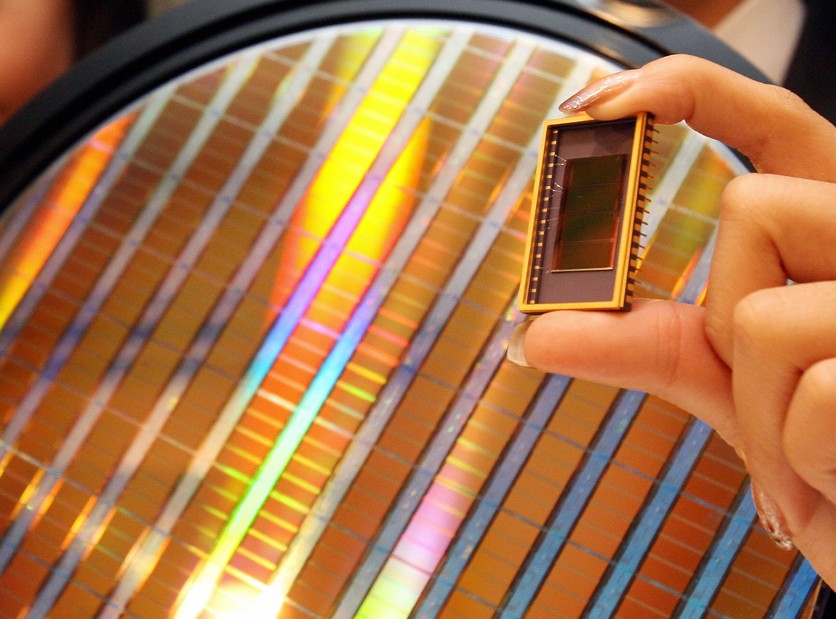
An employee of Samsung Electronics shows the world's first 30-nanometer 64-gigabit NAND flash memory device during a news conference in Seoul, 23 October 2007. KIM JAE-HWAN/gettyimages.com
Korean industry reports published this week confirmed what supply-chain analysts had flagged for months: Samsung has converted more than half of its most advanced commercial foundry node into a dedicated production line for its own high-bandwidth memory — and the companies that relied on that capacity for their own chip designs now find themselves, structurally and permanently, behind their own foundry's captive demand.
More than 15,000 wafers per month at Samsung's Pyeongtaek Campus 2 and Campus 3 facilities — produced on the S5 and S6 foundry lines running the company's 4nm SF4 FinFET process — are now routed internally to logic base dies for sixth-generation High-Bandwidth Memory 4, according to reports from ZDNet Korea and Digitimes, corroborated by TechPowerUp and Wccftech. The Digitimes report, published September 8, 2026, was confirmed by subscription-only access; the Wccftech report published September 7 is publicly available. Total 4nm monthly capacity at those facilities is approximately 30,000 wafers, meaning the internal allocation has reached 50 to 60 percent and the node is running at or near full utilization. The allocation is expected to hold through at least the end of 2026.
That figure is not a production bottleneck in the ordinary sense. It is a structural consequence of Samsung operating simultaneously as an integrated memory maker and as a foundry for external chip designers — and one is now eating the other.
When Your Foundry Is Also Your Competitor
To understand why fabless chip companies that design on Samsung's 4nm process face a different problem than customers of a pure-play foundry like TSMC, the distinction between an integrated device manufacturer and a contract foundry matters.
TSMC has no memory division, no internal chip products, and no captive demand for its own wafers. Every wafer TSMC starts goes to an external paying customer. When TSMC runs at full utilization, the constraint is shared symmetrically: every customer competes against every other customer on the open market, and price or priority determines who wins slots.
Samsung Foundry operates inside Samsung Electronics, a company that also designs and sells its own DRAM, HBM, and system-on-chip products. When Samsung's memory division needs logic base dies — as it increasingly does for HBM4 — it sources them from Samsung Foundry. That internal transaction does not go to market. It does not compete with external customers on equal terms. It simply takes capacity.
The result is that a fabless chip designer with a Samsung 4nm design win is not competing for wafers in a market. It is competing against its own foundry's highest-priority internal customer — Samsung's own memory business — which has both structural priority and the full weight of corporate strategy behind it. A design win at Samsung Foundry now comes with an implicit asterisk: available after internal demand is served.
Why HBM4 Requires a Leading-Edge Foundry Node
Previous generations of high-bandwidth memory — through HBM3E — used a base die that could be manufactured on less aggressive process nodes. HBM4 changes that equation, and understanding why explains why Samsung's memory division is now consuming so much of its own foundry's most valuable capacity.
HBM4 is a stacked architecture: multiple DRAM dies are physically bonded on top of a logic "base die" — a chip at the bottom of the stack that manages all the electrical connections, memory controllers, error-correction logic, and power delivery for the DRAM layers above it. Under the JEDEC JESD270-4 HBM4 standard, HBM4 doubled the interface width from the 1,024-bit bus in HBM3E to 2,048 bits and doubled the number of independent channels per stack from 16 to 32 — each divided into two pseudo-channels.
Those 32 channels, all managed by the logic base die, require a level of memory-controller complexity, power efficiency, and thermal handling that older process nodes simply cannot deliver at HBM4's required speeds of up to 13 gigabits per second per pin. Targeting 2.8 terabytes per second of bandwidth per stack — roughly more than double the throughput of HBM3E — demands a base die capable of sustaining that data rate without generating heat that would degrade the DRAM layers stacked above it. Samsung's answer is its 4nm FinFET foundry process, the same node that powers competing logic products.
Samsung pairs that 4nm base die with its own sixth-generation 10-nanometer-class DRAM process — called "1c" internally — for the memory dies themselves. That combination is why Samsung's HBM4 delivers 11.7 gigabits per second per pin consistently, approximately 46 percent higher than the 8 Gbps baseline set by the JEDEC specification.
The choice also produces a structural cost advantage. SK Hynix, Samsung's primary HBM rival, uses TSMC to fabricate its HBM base dies — a process that carries roughly a 30 percent manufacturing cost premium at that node compared to Samsung's in-house production. Samsung's vertical integration — designing, fabricating, and packaging the base die internally — eliminates that premium and gives Samsung direct control over the logic layer that governs its entire HBM4 stack's performance envelope.
What the Demand Engine Looks Like
The immediate cause of Samsung's factory transformation is the simultaneous ramp of multiple AI accelerator platforms — and Samsung is now a qualified supplier for all of them.
Nvidia's Vera Rubin platform, the successor to Grace Blackwell, entered full production after the GTC Taipei announcement on June 1, 2026. CEO Jensen Huang confirmed on June 5 that Samsung, SK Hynix, and Micron Technology have all qualified to supply HBM4 for Vera Rubin. Industry analysts estimated SK Hynix holds roughly 60 to 70 percent of the HBM4 volume for Vera Rubin systems, with Samsung at approximately 25 to 30 percent.
AMD's competing MI450 accelerator has also adopted HBM4, with reported configurations reaching high memory capacities. And in March 2026, Samsung secured an exclusive agreement to supply up to 800 million gigabits of 12-layer HBM4 to OpenAI for its custom AI chip, codenamed Titan — now shipping under its production name, Jalapeño, which OpenAI unveiled publicly on June 24, 2026. That deal accounts for roughly 15 percent of Samsung HBM4 output, making OpenAI the third-largest HBM4 customer after Nvidia and AMD.
The Jalapeño chip is being co-developed with Broadcom, manufactured by TSMC using the 3nm process node, and relies entirely on Samsung's HBM4 for its memory layer — meaning Samsung supplies the memory to a chip whose logic die is made by its primary competitor.
Samsung's Competitive Recovery
The scale of the manufacturing pivot reflects how dramatically Samsung's position in the HBM market shifted in a single year. In Q2 2025, Samsung held just 15 percent of the global HBM market by revenue, having stumbled through qualification difficulties with its HBM3E product for Nvidia's demanding specifications. SK Hynix dominated with 64 percent.
By Q2 2026, Samsung's HBM share reached 33 percent, according to Counterpoint Research data published September 3, 2026, while SK Hynix's share declined to 50 percent. Samsung was the only major supplier to grow its share in that quarter. Counterpoint Research said it expects Samsung's share to increase further as HBM4 shipments ramp through the second half of the year.
The comeback was powered by Samsung's successful mass production of HBM4, which began in February 2026 — the industry's first — and by the major customer qualifications that followed. By early August, Samsung HBM4 yield reached 80 percent, well ahead of the year-end target the company had set for itself, meaning fewer wasted wafer starts and a lower per-unit cost for every stack Samsung ships.
The recovery has also been lucrative. Demand for HBM4 logic dies surged alongside shipment volumes, and Samsung has reportedly raised prices for those dies by around 40 to 50 percent since the start of 2026, according to Financial News Korea and DealSite, corroborated by TrendForce. The 4nm node running at full capacity gives Samsung pricing leverage it did not have when foundry utilization was below 50 percent in late 2024.
Samsung has also raised broader advanced foundry prices — by up to 15 percent externally for 4nm customers — as TSMC simultaneously raised its sub-5nm prices by 5 to 10 percent, giving Samsung pricing room under the market leader while still extracting higher margins.
What Fabless Customers Face
The strategic consequences extend beyond Samsung's balance sheet. With more than half of Samsung's most advanced commercial node now serving an internal customer rather than the open foundry market, the pool of 4nm capacity available to third-party chip designers has meaningfully compressed.
This compression differs from the general tightness at TSMC in one important respect: TSMC's capacity constraints arise from universal market demand. Samsung's constraints arise partly from a deliberate internal reallocation — one that placed its own memory division at the front of the queue. An external Samsung Foundry customer with a multi-year agreement has no structural guarantee that internal HBM demand won't continue to grow and consume an even larger share of available capacity.
The situation adds pressure to an already tight global supply of sub-5nm manufacturing. TSMC's 5nm and 4nm capacity is also reported to be fully utilized through the end of 2026, with AI accelerator customers competing against smartphone SoC suppliers for every available wafer slot. Samsung's self-directed reallocation compresses what was already a narrow set of alternatives for fabless chip companies building at the leading edge.
What Comes Next
The current capacity configuration is not a temporary pivot. Samsung has indicated that HBM4E — an enhanced variant built on the same 4nm base die process and its own 1c DRAM, targeting 3.6 terabytes per second of bandwidth at up to 16 gigabits per second per pin — is on track for mass production before the end of 2026. Since HBM4E shares the same 4nm foundry process as HBM4, any transition to the next generation simply extends rather than relieves the internal demand on the node.
The allocation through the second half of 2026 looks durable, anchored by Nvidia's Vera Rubin production ramp, AMD's accelerator demand, and the OpenAI Jalapeño supply commitment. Whether Samsung continues gaining HBM market share from SK Hynix will depend on execution at the 4nm node — both yield performance and the pace at which HBM4 volumes become visible in shipment data. Counterpoint Research's September 2026 data showed Samsung was the only major supplier to grow its HBM revenue share in Q2, and the company's own executives said they expect HBM4 to exceed 60 percent of Samsung's total HBM revenue in the second half.
For a chipmaker that was fighting for foundry relevance less than two years ago, the transformation is complete enough to reshape a market. The question for Samsung's remaining external foundry customers is whether they are tenants in a fab that has found a better use for the space — or partners in a business that simply needs them less than it used to.
Frequently Asked Questions
Why does HBM4 need a 4nm foundry process when older HBM generations did not?
HBM4 substantially raised the engineering requirements for the logic base die at the bottom of each memory stack. The JEDEC JESD270-4 standard doubled the memory interface width to 2,048 bits and doubled the channel count to 32 — each managed by the base die's memory controllers, power delivery circuits, and error-correction logic. Running that controller logic at up to 13 gigabits per second per pin without generating excess heat in a densely stacked assembly requires the power efficiency and transistor density that only an advanced logic process like 4nm can reliably deliver. Earlier HBM generations used base dies built on less aggressive nodes because the bandwidth targets were lower and the controller complexity was correspondingly smaller.
What does Samsung's internal 4nm allocation mean for companies that design chips at Samsung Foundry?
External Samsung Foundry customers designing chips on the 4nm node are now competing for a smaller pool of available wafers than they were a year ago — and the customer consuming the other half of that node is Samsung's own memory division. Unlike tightness at a pure-play foundry like TSMC, where all customers compete on equal market terms, Samsung's internal allocation reflects a corporate priority decision that external customers cannot negotiate around. Companies with existing Samsung 4nm design wins should factor in the possibility that internal HBM demand will continue to grow; those evaluating where to tape out next-generation designs should weight TSMC's 5nm-class nodes against Samsung's 4nm availability with that structural constraint in mind.
How does Samsung's in-house base die production compare to SK Hynix's approach?
Samsung fabricates its HBM4 base dies internally on its own 4nm foundry process, while SK Hynix sources its HBM base dies from TSMC. That outsourcing arrangement carries roughly a 30 percent manufacturing cost premium at the same process node — a structural cost disadvantage built into every HBM stack SK Hynix ships. Samsung's vertical integration also gives it direct control over the logic layer's design and yield optimization, without depending on an external foundry partner's scheduling or qualification cycles. The tradeoff is that Samsung's foundry arm serves as both a contract manufacturer for external customers and the captive supplier for its own memory business — a dual role that is now visibly compressing external access to the node.
Is OpenAI's custom AI chip, Jalapeño, now the third-largest consumer of Samsung HBM4?
Yes, by volume allocation. The March 2026 agreement between Samsung and OpenAI committed up to 800 million gigabits of 12-layer HBM4 for the second half of 2026 — approximately 15 percent of Samsung's specific HBM4 production capacity for the year. That makes OpenAI the third-largest HBM4 customer by volume allocation, behind Nvidia and AMD. The Jalapeño chip, co-developed with Broadcom and manufactured by TSMC on a 3nm process, relies entirely on Samsung's HBM4 for its memory layer — an arrangement that adds another committed block of Samsung's internal foundry output to the allocation that has already filled the 4nm node.

-
 C114 Communication Network
 -
 Communication Home
