
 Search

Kioxia.com
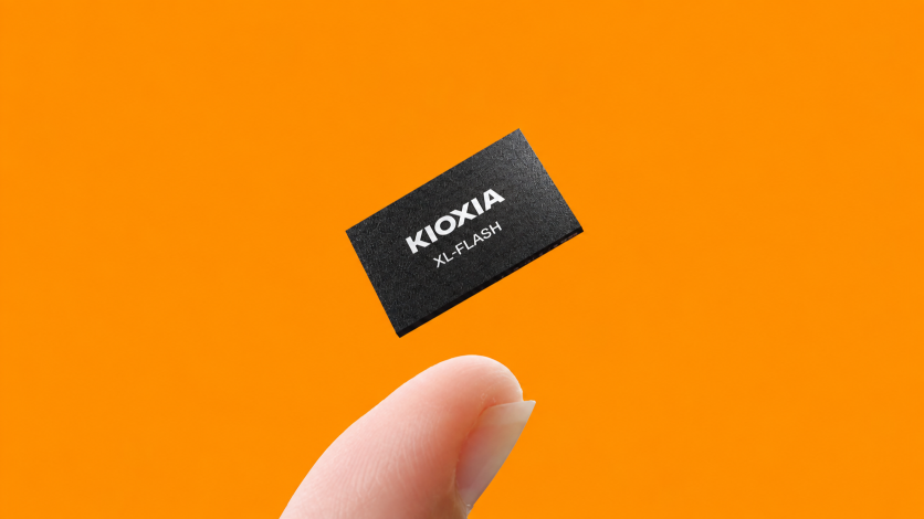
Kioxia has confirmed that its next-generation XL-Flash Gen 3 storage class memory, paired with the PCIe 7.0 interface, will target 100 million random read IOPS by 2028 — a one-year slip from the company's earlier 2027 goal, driven not by a problem with the flash silicon itself but by the time it takes for the PCIe 7.0 ecosystem to complete certification. For AI infrastructure architects planning data center buildouts, that distinction matters: Kioxia is not waiting on its own technology. It is waiting on the rest of the industry to certify the interface that makes 100 million IOPS physically deliverable.
The company's first-generation entry in this architecture, the GP1 Series SSD, reached evaluation-sample status at FMS 2026 in Santa Clara on August 4. The GP1 delivers 10 million random read IOPS at a 512-byte block size using second-generation XL-Flash over a PCIe 6.0 interface — earning the FMS Best of Show award in the Specialized Storage category. The jump to 100 million IOPS comes in the drive generation after that, built on XL-Flash Gen 3 and the PCIe 7.0 interface — and why 2028 is the target has everything to do with when PCIe 7.0 platforms will actually be certifiably available.
From 10 Million to 100 Million: Why the Gap Is an Architecture Problem, Not Just a Speed Target
The tenfold IOPS jump from GP1 to the Gen 3 drive is not a single engineering problem; it is the intersection of three constraints that all must be solved simultaneously: the flash memory's internal parallelism, the controller architecture, and the host interface bandwidth.
Kioxia has disclosed that XL-Flash Gen 3 triples read performance of Gen 2 silicon and delivers 150 percent higher write performance. Those gains come from the same levers the company has pulled in prior XL-Flash generations: shorter word lines and bit lines to reduce the RC delay that limits how quickly a cell can be read, and a higher count of parallel planes per die to allow more simultaneous read operations. Kioxia currently achieves 16 planes per die in XL-Flash Gen 2, compared to three to six in conventional consumer NAND — more planes mean more read operations firing in parallel on each die, which is what drives the sub-5-microsecond read latency and the 10-million-IOPS figure that GP1 achieves today.
Energy efficiency is improving, but the gains lag the performance jump. Kioxia projects a 40 percent improvement in read energy efficiency for Gen 3, and 80 percent for writes. Against a 3× performance increase, that means each individual IOPS consumes roughly twice the energy it did in Gen 2. Dense GPU pod deployments running Gen 3 drives will need liquid cooling — a technology Kioxia has already introduced on the GP1 and its CM10 enterprise SSD lineup — to manage thermal density at these power levels.
The PCIe interface constraint is where 2028 becomes the governing date. At 10 million IOPS with 512-byte blocks, GP1 moves approximately 5 gigabytes of data per second — using only about 15 percent of a PCIe 6.0 x4 link's capacity. The interface has plenty of headroom. At 100 million IOPS, the math changes: 100 million operations times 512 bytes equals roughly 51 gigabytes per second. A PCIe 7.0 x4 link at 128 gigatransfers per second provides about 64 gigabytes per second of usable bandwidth — enough to carry the full load with a modest margin. A PCIe 6.0 x4 link at 64 gigatransfers per second provides about 32 gigabytes per second — only 60 percent of what 100 million IOPS requires. PCIe 7.0 is a physical requirement for Gen 3; it is not a preference.
PCIe 7.0 Compliance Is the Clock That Kioxia Cannot Control
PCI-SIG finalized the PCIe 7.0 specification in June 2025. But a finalized spec is not a certifiable ecosystem. PCI-SIG's compliance program timeline — the process by which host controllers, drives, and platforms are verified to interoperate correctly — runs on its own schedule after spec release. Preliminary compliance testing is scheduled for 2027, with the official Integrators List (the published register of certified PCIe 7.0 hardware) scheduled for 2028.
That 2028 certification date is exactly why Kioxia slipped its 100-million-IOPS target by a year. Without certified PCIe 7.0 host platforms shipping to data center customers in volume, Kioxia cannot ship the drive at commercial scale into deployments that can actually use it. The company had originally indicated a 2027 hardware target based on an earlier reading of the PCIe 7.0 ecosystem timeline; the 2028 date reflects alignment with the actual certification roadmap.
Commercial PCIe 7.0 devices and platforms are not broadly expected before 2028 at the earliest. The one-year slip in Kioxia's roadmap is therefore a calibration of its own schedule to the industry's, not a signal that the memory engineering is behind.
What XL-Flash Is — and Why Standard NAND Cannot Do This Job
XL-Flash is not conventional NAND. Every mainstream enterprise SSD — from read-intensive data center drives to the highest-performance TLC NVMe drives — uses multi-level cell technology that stores multiple bits per transistor: three bits per cell for TLC, four for QLC. Multi-level storage is what enables enterprise SSDs to hold tens of terabytes on a handful of chips. But each additional bit per cell makes the cell harder and slower to read: a TLC read requires multiple sensing steps that push latency to the 50-to-100-microsecond range and limit parallel access rates.
XL-Flash uses SLC (single-level cell) mode — one bit per cell — sacrificing density for a fundamental physics advantage. With only two voltage states to distinguish instead of eight, an SLC cell can be read in a single sensing operation with read latencies under five microseconds. That is 10 to 20 times lower latency than standard enterprise NAND. Combined with 16 planes per die operating in parallel, XL-Flash Gen 2 achieves the 10-million-IOPS figure GP1 demonstrates. XL-Flash Gen 3 raises the per-die plane count and shortens the word-line geometry further to reach the 3× performance target.
The access granularity is the other critical distinction. Standard enterprise SSDs operate on 4-kilobyte or larger block sizes — sensible for sequential workloads like loading model weights or writing training data. XL-Flash operates at 512-byte granularity, roughly the size of a single attention vector during AI inference. That fine-grained access is what makes XL-Flash suitable for key-value cache management, where the AI model issues thousands of random reads per second at precisely this scale as it retrieves cached attention states from prior conversation turns.
SLC NAND also offers dramatically higher endurance. XL-Flash Gen 2 sustains between 150,000 and 250,000 program-erase cycles per cell, compared to roughly 3,000 for TLC. KV cache workloads write constantly — each inference turn updates the cache — making high endurance as important as high IOPS. GP1 is rated for up to 50 drive writes per day, roughly 50 times the endurance rating of a typical read-intensive enterprise SSD.
The AI Memory Problem That XL-Flash Gen 3 Is Designed to Solve
Large language models generate an intermediate attention memory called the key-value cache during inference. When a model processes a long conversation or a document, it stores the intermediate computational results for each prior token so it does not have to reprocess them on every new output. For a 70-billion-parameter model handling a million-token context window, a single user's KV cache can exceed 320 gigabytes — four times the entire high-bandwidth memory capacity of an Nvidia H100 GPU.
At that scale, KV cache cannot live in GPU memory alone. It must spill to an adjacent storage tier. Flash storage at PCIe-attached latency is the practical candidate: close enough to the GPU to be accessible quickly, cheap enough per gigabyte to be economically viable, and durable enough to handle the constant write churn of cache updates. The GP1's role in Nvidia's Storage-Next initiative is precisely this: providing an overflow tier for GPU high-bandwidth memory that is fast enough to avoid stalling inference.
At 100 million IOPS, an XL-Flash Gen 3 drive on a PCIe 7.0 link would deliver data at a rate and granularity where flash storage becomes genuinely competitive with lower tiers of HBM for KV cache retrieval specifically — not for model-weight loading, where sequential bandwidth matters more, but for the random-access, small-block retrieval pattern that KV cache management demands. High-bandwidth memory remains the gold standard for raw bandwidth and latency, and costs far more per gigabyte than flash. The economic pressure on AI data center operators to offload even moderately warm KV cache data to a flash tier is already significant, and 100 million IOPS makes that offload more viable.
Storage-Next Is the Ecosystem Kioxia Is Building Into
The GP1 did not debut as a standalone product. It arrived as part of Nvidia's Storage-Next initiative, a formal industry coalition of more than 40 storage and flash vendors — including Google, Intel, Meta, Micron, and DDN — aligned around standardizing how GPU-driven storage should behave when thousands of GPU threads issue simultaneous small random reads. The Storage-Next coalition aligns GPU storage standards across more than 40 vendors.
At FMS 2026, Nvidia deepened this infrastructure. The company open-sourced cuFile APIs to GitHub — the software library that enables GPUs to initiate storage reads without CPU involvement — with Google, Intel, and Meta as inaugural maintainers on a neutral GitHub repository. Separately, Nvidia presented SCADA as productized accelerated storage access — the productized form of its earlier Big Accelerator Memory research — as the framework for coordinating GPU-initiated storage requests across massively parallel inference pipelines.
The combined picture is of an open-standard infrastructure stack being assembled specifically for the GPU-to-flash data path that XL-Flash Gen 3 will operate within. Kioxia is not building to a proprietary Nvidia interface; it is building to an open, multi-vendor standard whose ecosystem will be ready — and certified — in 2028.
Kioxia Is Not the Only Team in This Race
On August 4, 2026, the day FMS opened, SK Hynix and SanDisk published the first HBF technical specification through the Open Compute Project. High Bandwidth Flash takes a different architectural approach to the same problem: instead of attaching flash at the end of a PCIe link like Kioxia's GP1, HBF stacks NAND dies using through-silicon vias and connects to accelerators via UCIe, the open chiplet interconnect standard. The specification covers configurations up to 512 gigabytes per device, with three bandwidth grades running from approximately 0.4 terabytes per second to 3.0 terabytes per second.
The two approaches are not directly substitutable. Kioxia's PCIe-attached SSD design requires no new die-stacking or packaging infrastructure beyond what PCIe 7.0 platforms will provide. High Bandwidth Flash requires accelerator vendors and system integrators to adopt new packaging and interconnect standards at the chip level. PCIe-attached flash is easier to integrate at volume in the near term; HBF offers higher potential bandwidth density per device if the packaging ecosystem matures.
Kioxia has not committed exclusively to the PCIe-attached approach. The company also exhibited an XL-Flash-based CXL memory expansion module — the XL1 — with evaluation samples shipped to ecosystem partners in August 2026. And Kioxia has its own TSV-stacked high-bandwidth flash effort, with Nvidia driving partner discussions. Three architectural positions in the AI memory hierarchy simultaneously — on the accelerator package, on the memory bus via CXL, and at the end of a PCIe link — is a hedge against an architecture race that remains unsettled.
An oddity worth noting: Kioxia and SanDisk jointly operate the Yokkaichi and Kitakami NAND fabrication facilities in Japan under a long-standing joint venture. The NAND chips SanDisk will use in HBF and the chips Kioxia will use in XL-Flash Gen 3 flow from the same production lines. Two companies are backing competing architectures for the same emerging AI memory tier out of shared wafer capacity.
Read more: Kioxia NAND Flash Mass Production Accelerates: BiCS10 Target Puts Samsung and SK hynix on Edge
What Buyers and Infrastructure Teams Should Take Away
The GP1's arrival by end of 2026 — with evaluation samples shipping to select enterprise customers on Kioxia's stated schedule — gives infrastructure architects a working, purchasable implementation of the Storage-Next flash tier today. At 10 million IOPS and sub-5-microsecond latency in the EDSFF E1.S and E3.S form factors, with cold-plate liquid cooling support on select variants, the GP1 is ready for qualification in Nvidia CMX-compatible AI server deployments.
The XL-Flash Gen 3 drive at 100 million IOPS is a 2028 event whose timeline is governed by the PCIe 7.0 ecosystem certification schedule, not by Kioxia's silicon. That distinction is what Kioxia SVP Neville Ichhaporia framed at FMS 2026: "The AI memory wall is a critical challenge for our industry to solve on the way to growing the scale and capability of AI deployment." The GP1 is the industry's first answer to that wall at 10 million IOPS. XL-Flash Gen 3 is the architecture's answer at 100 million.
Whether 2028 holds will depend on factors Kioxia does not control: PCIe 7.0 controller silicon from AMD, Intel, and Nvidia reaching the Integrators List on schedule; server platform certification; and the readiness of the Storage-Next ecosystem to support GPU-initiated direct storage access at scale. The slip from 2027 to 2028 is a reminder that even well-funded roadmaps are governed by the slowest element in the ecosystem they depend on. For AI infrastructure planners, the implication is practical: invest in GP1-class PCIe 6.0 flash now for current 10-million-IOPS workloads, and plan the 100-million-IOPS infrastructure upgrade on a 2028 horizon.
Frequently Asked Questions
What is XL-Flash, and how does it differ from the NAND inside a standard enterprise SSD?
XL-Flash is Kioxia's single-level cell (SLC) storage class memory — it stores one bit per transistor rather than the three or four bits per cell that TLC and QLC NAND use. That single-bit design allows read operations in under five microseconds (compared to 50-100 microseconds for TLC), supports 512-byte access granularity rather than the 4-kilobyte blocks standard SSDs use, and sustains 150,000 to 250,000 program-erase cycles per cell rather than TLC's roughly 3,000. The tradeoff is density: an XL-Flash drive holds far less data per unit of chip area than a TLC drive of the same physical size. For AI inference's KV cache workloads — which need fast random reads of small blocks, constantly updated — XL-Flash's speed and endurance profile is the correct engineering choice even at the cost of capacity.
Why was the 100-million-IOPS target pushed from 2027 to 2028?
Kioxia's XL-Flash Gen 3 silicon is on track; the delay is an ecosystem problem, not a memory problem. At 100 million IOPS times 512 bytes, the drive must move roughly 51 gigabytes of data per second — more than a PCIe 6.0 x4 link can carry. PCIe 7.0 at 128 gigatransfers per second is physically required for 100M IOPS, not just preferred. PCI-SIG finalized the PCIe 7.0 specification in June 2025 but has scheduled preliminary compliance testing for 2027 and official interoperability certification for 2028. Without certified PCIe 7.0 host platforms available in the market, Kioxia cannot ship the drive into data center deployments at scale. The 2028 date aligns with when that certification infrastructure will exist.
What is Nvidia's Storage-Next initiative, and how does Kioxia's GP1 fit into it?
Storage-Next is an Nvidia-led GPU storage initiative of more than 40 storage and flash vendors — including Kioxia, Micron, DDN, Google, Intel, and Meta — aligned around standardizing how GPU-driven storage should behave. The initiative's premise is that GPU high-bandwidth memory alone cannot hold the key-value caches and working datasets that modern AI inference requires, and that flash storage must become a first-class participant in the GPU memory hierarchy rather than a passive recipient of CPU-managed writes. Nvidia open-sourced its cuFile APIs enabling GPU direct storage at FMS 2026 to enable GPU-initiated direct storage reads without CPU involvement, and introduced its SCADA framework for coordinating those reads at scale. The GP1 is Kioxia's first Storage-Next-aligned drive: purpose-built for GPU direct access, rated for 10 million IOPS at 512-byte granularity, and designed as the first step in a roadmap that reaches 100 million IOPS in 2028.
How does the Kioxia GP1's approach differ from the High Bandwidth Flash standard that SK Hynix and SanDisk announced at FMS 2026?
The GP1 attaches to GPUs via a standard PCIe 6.0 interface — the same bus that connects any NVMe SSD. No new packaging standards, no new chiplet interconnects, no new accelerator designs required. High Bandwidth Flash, announced through the Open Compute Project by SK Hynix and SanDisk at FMS 2026, stacks NAND dies vertically using through-silicon vias and connects to accelerators via UCIe — the open chiplet interconnect — delivering up to 512 gigabytes per device and up to 3 terabytes per second of bandwidth. HBF offers higher bandwidth density but requires new accelerator packaging and interconnect adoption that PCIe-attached drives do not. The two approaches are competing answers to the same question — how to put more fast flash closer to GPU compute — and the market has not yet determined which architecture will dominate.

-
 C114 Communication Network
 -
 Communication Home
