
 Search

Skhynix.com
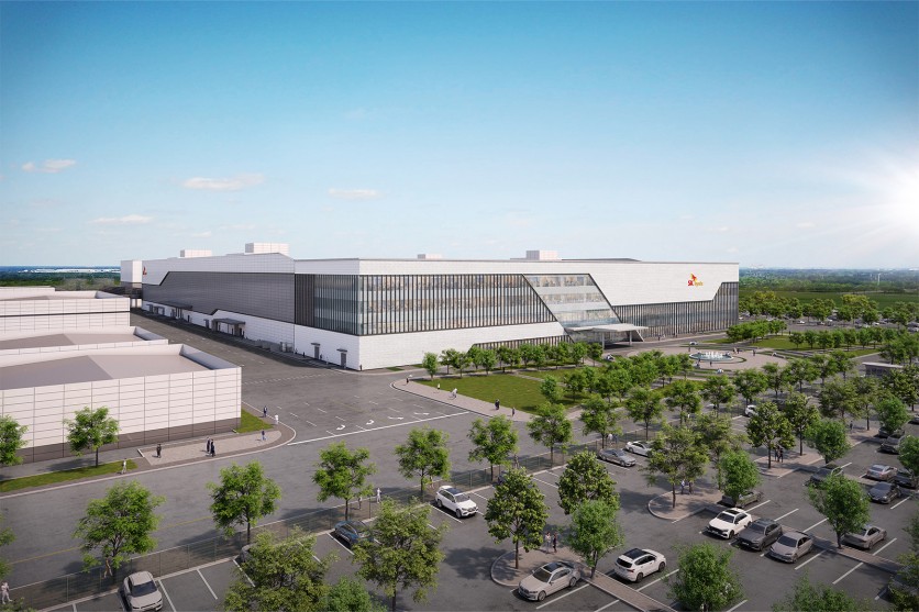
South Korean memory giant SK Hynix officially broke ground on its more than $4 billion advanced packaging facility at Purdue Research Park in West Lafayette, Indiana, on August 27, opening what the company calls the United States' first dedicated high-bandwidth memory production hub — and the CEO who presided over the ceremony told reporters that the global memory shortage driving the investment will not relent until at least the end of 2030.
CEO Kwak Noh-Jung said at the event that he has observed no meaningful indicators of a coming memory-cycle decline, and that any eventual softening would involve a gradual moderation in demand rather than the sharp, cyclical collapses that have historically punished the memory industry. The forecast landed the day after Nvidia — SK Hynix's most strategically important customer — projected a 70% revenue jump for its coming fiscal year, reinforcing confidence in the durability of AI spending that has fueled demand for every high-bandwidth memory chip SK Hynix can make.
What America's First HBM Hub Will Actually Do
The Indiana facility is an advanced packaging and testing operation — not a chip fabrication plant in the traditional sense, and that distinction matters for understanding what the groundbreaking actually delivers.
When engineers talk about making a semiconductor, they typically mean two separate phases. Front-end fabrication is where blank silicon wafers are transformed into functioning memory dies through hundreds of photolithography, deposition, and etch steps, using some of the most precise manufacturing equipment ever built. Back-end packaging is where those finished dies are assembled, interconnected, stacked, and tested to produce a functional product.
The Indiana facility handles the back-end. Cutting-edge DRAM wafers manufactured at SK Hynix's facilities in Icheon and Yongin, South Korea, will be shipped to West Lafayette, where they will undergo the stacking, interconnection, and testing steps required to produce finished HBM modules. No memory cell will be fabricated on American soil. What will happen in Indiana is something the United States does not currently do at all: assemble high-bandwidth memory from start to finish, test it to production quality, and ship it to US AI accelerator customers from a domestic address.
How Advanced Packaging Turns Korean Wafers Into AI Fuel
The specific packaging process SK Hynix will perform in Indiana is technically demanding in ways that standard assembly operations are not.
First, each DRAM die arriving from Korea is ground down to near-transparent thickness — thin enough for vertical electrical connections to pass through it. Engineers then drill through-silicon vias at microscopic pitch through each die, creating the vertical channels that allow individual memory layers to communicate at speeds impossible with horizontal wiring. The thinned dies are then stacked up to 12 layers high. SK Hynix uses its proprietary Mass Reflow Molded Underfill (MR-MUF) bonding process during stacking, injecting a liquid protective compound between layers as they are fused — a step that both improves thermal performance and protects the assembly from mechanical stress.
The finished HBM stack, once tested, will then be shipped to TSMC's facilities — primarily its Arizona campus — where it will be placed on a silicon interposer alongside Nvidia's GPU die and the two components will be bonded together through TSMC's Chip on Wafer on Substrate (CoWoS) process. That bonded assembly is what ends up inside Nvidia's AI accelerators. The Indiana facility handles the HBM side of that equation.
The cleanroom where this work will happen is targeted to open by October 2028. Volume production of next-generation HBM4E chips — the standard that will power AI accelerators in the 2029–2030 window — is scheduled to begin in the third quarter of 2029.
What Indiana Closes — and What It Does Not
The groundbreaking is a genuine milestone. Until now, every high-bandwidth memory chip reaching an Nvidia GPU, a Microsoft Azure server, or a Google data center has been packaged in East Asia — a logistical and geopolitical dependency that US policymakers have flagged for years. The Indiana facility changes that, creating a domestic supply point that reduces shipping time, insulates the HBM supply chain from specific kinds of geopolitical disruption, and gives US-based hyperscalers a source of supply that meets CHIPS Act domestic content requirements.
What it does not change is where the underlying memory dies come from. If Korean wafer production were disrupted — by a natural disaster, a trade escalation, or a supply chain incident — the Indiana packaging plant would have nothing to assemble.
That gap is precisely what Washington is now pressing to fill. US Commerce Secretary Howard Lutnick has publicly told Samsung and SK Hynix that they will "have no choice" but to commit to front-end memory wafer fabrication on American soil — the process that would manufacture actual DRAM dies in the United States, not merely assemble Korean-made ones. SK Hynix has confirmed it is actively scouting potential US sites for such a facility, with Chairman Chey Tae-won stating the company is open to building one "if key conditions are met" regarding power, water, workforce, and supply chain infrastructure.
SK Hynix's board this month approved approximately ₩54.3 trillion (approximately $39.5 billion at current exchange rates) in capital investment through 2031, the bulk of which is directed at expanding South Korean fab capacity at Yongin — underscoring that Indiana is a complement to the Korean production base, not a move toward replacing it.
Kwak's Market Forecast: The Shortage Doesn't End Here
The memory cycle that has driven unprecedented demand for SK Hynix's products — and made the Indiana investment commercially rational — is not expected to ease until well into the next decade, by Kwak's account.
SK Hynix currently holds a commanding 58% of global HBM revenue as of the first quarter of 2026, according to Counterpoint Research, with Samsung Electronics and Micron Technology each holding approximately 21%. The company has confirmed that its entire production capacity for DRAM, NAND, and HBM is fully committed through 2026 — an extraordinary degree of forward visibility driven by long-term agreements with customers including Nvidia, Microsoft, and Alphabet's Google.
Kwak said at the ceremony that after 2030, he expects supply and demand to "become more balanced," while the AI industry continues to grow. That framing is meaningfully different from a prediction of a downturn: Kwak is describing a transition from severe shortage to equilibrium, not a bust cycle.
The record $26.5 billion Nasdaq listing SK Hynix completed in July — the largest-ever US listing by a foreign company — has given American investors direct exposure to that shortage-driven revenue, further deepening the strategic logic of a visible US manufacturing commitment.
The Nvidia Partnership That Makes Indiana Strategically Necessary
The timing and framing of the Indiana groundbreaking are inseparable from the Nvidia-SK Hynix multiyear technology partnership announced jointly on June 7, 2026. Under that agreement, the two companies committed to co-developing next-generation memory across Nvidia's full product roadmap — including the Vera Rubin AI supercomputer platform, Vera CPUs, RTX Spark personal AI computers, and Jetson Thor robotics platforms.
Jensen Huang, Nvidia's founder and CEO, said at the partnership announcement that SK Hynix has been an "extraordinary partner" and that together the companies will "codevelop the next generation of memory for AI factories."
The Indiana facility operationalizes that relationship for the US market: instead of shipping finished HBM modules from Korea to US customers, SK Hynix will be able to deliver domestically packaged, domestically tested HBM directly to data centers in California, Texas, and wherever Nvidia's American customers are building their AI infrastructure. Kwak called Indiana "a gateway to deliver the first Made-in-USA HBM products" and said the company intends to grow its US investments and "become the most trusted partner in shaping the future of AI in America."
Ceremony, Community, and the Korea-US Alliance Dimension
The August 27 groundbreaking was held at the Holloway Gymnasium on Purdue University's campus, attended by Indiana Governor Mike Braun, US Senator Todd Young, Purdue University President Mitch Daniels, South Korean Ambassador Kang Kyung-wha, and Chairman of the Korea-US Alliance Foundation Robert Abrams, alongside SK Hynix's CEO and two Vice Chairmen.
Senator Young, who was a primary architect of the CHIPS and Science Act that provided up to $458 million in grants and $500 million in loans — finalized under the CHIPS program in December 2024 — for the project, called the investment "further proof that Indiana is leading the way in rebuilding America's semiconductor industry." Governor Braun said the project would "usher in the next generation of American innovation" and bring "thousands of good-paying jobs to Indiana."
Beyond the production lines, the facility will include an "Advanced Packaging R&D Testbed" that customers, universities, and technology partners can use to co-develop next-generation packaging technologies and run prototype fabrication at speed — a capability that positions the Indiana campus as an ecosystem hub, not merely a production site.
SK Hynix also announced at the ceremony that it signed a Purdue University research MOU covering joint research on system integration and advanced packaging technologies, with plans to recruit graduate talent from across the Midwest. In a separate move recognizing the historical connection between Indiana and Korea — Indiana contributed approximately 140,000 troops during the Korean War — SK Group agreed to provide jobs for discharged USFK veterans through the Korea-US Alliance Foundation's veterans job platform.
The overall investment is projected to sustain roughly 7,000 total jobs in the region — counting construction, commercial operations, and supplier activity — with approximately 1,000 direct employees during active production. The facility spans 133.5 acres (54 hectares) of Purdue Research Park, making it the largest single development project in Indiana history.
Read more: Washington Demands Samsung, SK Hynix Build US Memory Fabs After Korea's $577B Chip Bet
Does the US Make HBM Chips Domestically Now?
Not yet — and not after this facility opens, in the strict sense. The Indiana plant will package and test HBM chips assembled from wafers manufactured in South Korea. No DRAM or HBM wafer fabrication currently occurs on American soil, and the CHIPS Act's existing investments do not include funding for front-end memory wafer manufacturing. Micron Technology, the only US-headquartered HBM producer, fabricates its HBM wafers in Hiroshima, Japan, and packages them in Taichung, Taiwan. What changes with Indiana is the final assembly and testing step — which is where "Made in USA" applies in a meaningful commercial and regulatory sense, and where approximately half of the total product value is created. Front-end HBM wafer fabrication in the US, if it happens, is a separate story that will require new commitments from SK Hynix or competitors — and Washington is actively pushing for exactly that.
Currency conversions in this article are approximate and based on exchange rates as of August 30, 2026.
Frequently Asked Questions
What is the difference between advanced HBM packaging and wafer fabrication, and why does it matter?
Wafer fabrication — the "front end" — is where blank silicon wafers are transformed into functioning memory dies using photolithography, chemical deposition, and etching in clean rooms equipped with extreme ultraviolet lithography tools. Advanced packaging — the "back end" — takes those finished dies and stacks, interconnects, and tests them into completed products. SK Hynix's Indiana facility handles the back end: it receives DRAM wafers manufactured in South Korea and produces finished HBM modules for delivery to US customers. This means the facility is the first of its kind on American soil and creates a meaningful domestic supply point, while the underlying silicon memory dies will continue to be manufactured in Korea for the foreseeable future. Washington's demand for "front-end memory fabs" is a separate ask that the Indiana investment does not fulfill.
When will SK Hynix's Indiana facility actually start producing HBM chips?
The cleanroom is targeted to open by October 2028, after which initial production runs and customer qualification testing will begin. Volume production of next-generation HBM4E chips — the standard expected to power AI accelerators in the 2029–2030 technology cycle — is scheduled to begin in the third quarter of 2029. SK Hynix's CEO has stated the company's goal is for Indiana to become a key US HBM production base by 2030.
What does CEO Kwak's memory shortage forecast mean for AI chip prices and supply in the near term?
Kwak's on-the-record statement at the groundbreaking is that the global HBM shortage will persist through the end of 2030, with demand moderating gradually after that rather than collapsing in the sharp cycles that have historically characterized memory markets. For buyers — AI infrastructure operators, hyperscalers, enterprise IT teams — this means continued tight supply and pricing pressure on HBM-dependent systems well into 2029. The Indiana facility will not meaningfully change that picture before its Q3 2029 production ramp; its contribution to supply will arrive roughly at the point the market is expected to shift toward equilibrium. For AI startups and mid-tier cloud providers without multi-year supply agreements, the shortage environment Kwak described will remain an operating constraint for the next three-plus years.
How is the Indiana plant connected to the US-South Korea semiconductor trade relationship?
The $458 million in CHIPS Act grants and $500 million in federal loans that helped fund the Indiana plant are part of a broader US policy effort to reduce dependence on East Asian semiconductor supply chains and incentivize Korean and Taiwanese chipmakers to establish US production capacity. SK Hynix's commitment deepens economic ties between the two countries — illustrated at the groundbreaking by the USFK veterans employment program and the Purdue University research partnership. At the same time, Washington is separately pressing SK Hynix and Samsung to go further, committing to front-end memory wafer fabrication on American soil — a request that SK Hynix is actively evaluating but has not yet fulfilled.

-
 C114 Communication Network
 -
 Communication Home
