
 Search

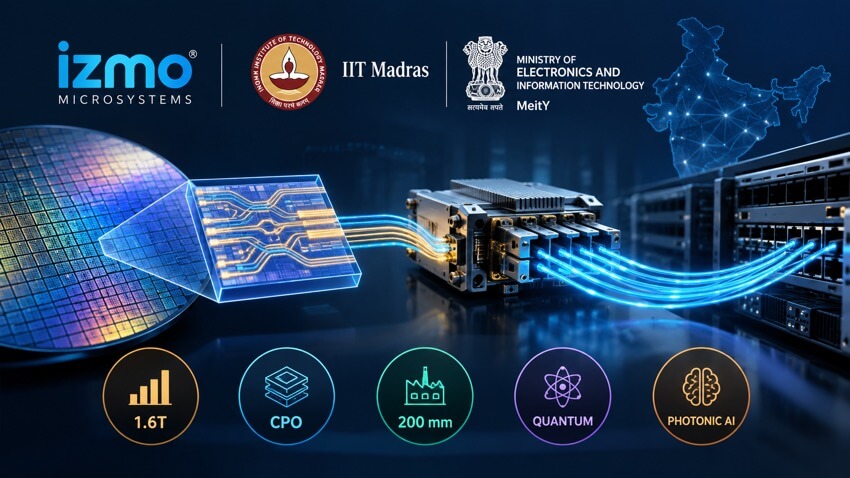
izmo Microsystems and the Indian Institute of Technology Madras (IIT Madras) are moving into Phase II of a five-year, government-backed silicon photonics initiative aimed at translating photonic integrated circuit research into deployable technologies for AI data centers, telecommunications, quantum communications and advanced computing. The Silicon Photonics Enabled Cutting-edge Technology Research and Applications program, or SPECTRA, has a total outlay of ₹99.94 crore (approximately $10.3 million), including ₹97.54 crore (approximately $10.1 million) from India’s Ministry of Electronics and Information Technology (MeitY) and ₹2.40 crore (approximately $247,000) in cash and in-kind support from izmo Microsystems.
SPECTRA represents Phase II of IIT Madras’ Centre for Programmable Photonic Integrated Circuits and Systems (CPPICS). The program will span PIC design, fabrication and characterization through advanced packaging, testing and system integration. Among its principal targets are a 1.6 Tbps silicon photonics transceiver engine operating at 1550 nm, microwave photonic engines operating beyond 50 GHz, integrated quantum random-number generation and quantum-key-distribution systems, and photonic processors for AI workloads. The program also calls for development of a silicon photonics Process Design Kit containing more than 100 IP blocks for 200 mm wafer platforms.
Official SPECTRA / CPPICS Phase II program page: https://cppics.iitm.ac.in/researcharea
For izmo Microsystems, the collaboration extends beyond chip design into the manufacturing challenges surrounding next-generation optical engines. The company is expected to work on packaging architecture, CPO interfaces, PIC-EIC co-integration, fiber alignment and attachment, process optimization, prototype assembly, production packaging and reliability validation. The five-year roadmap ultimately calls for a certified co-packaged optics design rule and service capability, establishing a path from photonic design and foundry fabrication through packaging, qualification and system-level deployment.
| SPECTRA Phase II — Key Points | |
| Program | Silicon Photonics Enabled Cutting-edge Technology Research and Applications (SPECTRA) |
| Investment | ₹99.94 crore (~$10.3M) over five years |
| MeitY Funding | ₹97.54 crore (~$10.1M) |
| izmo Commitment | ₹2.40 crore (~$247K) cash and in-kind |
| 1.6T Target | 1.6 Tbps silicon photonics engine at 1550 nm for HPC and data-center routing |
| CPO | PIC-EIC co-integration, fiber attachment, packaging, reliability validation and a certified CPO design rule/service capability |
| Process Ecosystem | 200 mm silicon photonics PDK with more than 100 IP blocks |
| Applications | AI data centers • CPO • quantum communications • photonic AI |
Dinanath Soni, Director of izmo Microsystems, said the transition from 400G and 800G toward 1.6T places increasing importance not only on photonic chip design but also on packaging, fiber attachment, electronic-photonic integration, thermal management and high-speed testing. The partnership combines IIT Madras’ silicon photonics research with izmo’s packaging and manufacturing capabilities to move prototypes toward production-ready modules and co-packaged optical systems.
Analysis
The significance of SPECTRA is its emphasis on the manufacturing stack surrounding silicon photonics rather than treating the PIC as an isolated technology. Moving from a functioning photonic die to a deployable 1.6T optical engine or CPO assembly requires repeatable fiber coupling, electrical-photonic integration, thermal management, packaging, test and reliability processes. These are increasingly important engineering constraints as optical interfaces move closer to switch and accelerator silicon.
The program also places India into a broader global effort to build domestic silicon-photonics design and manufacturing ecosystems. The proposed 200 mm PDK with more than 100 IP blocks is particularly relevant because a reusable process and design ecosystem can support multiple products rather than a single research prototype. The longer-term target of a certified CPO design rule and packaging service could give the program an industrial output extending beyond the specific 1.6T engine.
This is a material progression from izmo Microsystems’ September positioning around production-stage silicon-photonics packaging and its optical-transceiver roadmap. SPECTRA gives that manufacturing strategy a five-year R&D framework extending upstream into PIC design and process enablement and downstream into CPO integration and reliability. The critical milestones to watch will be whether the program converts its 200 mm design ecosystem, 1.6T engine and CPO packaging work into qualified devices and repeatable manufacturing processes.
| Company Profile — izmo Microsystems | |
| Company | izmo Microsystems Pvt. Ltd. |
| Headquarters | Bengaluru, India |
| Parent | izmo Limited (NSE: IZMO; BSE: 532341) |
| Key Leader | Dinanath Soni — Director |
| Focus | Advanced semiconductor packaging and manufacturing |
| Technologies | Silicon photonics • CPO • SiP • heterogeneous integration • RF/microwave packaging |

-
 C114 Communication Network
 -
 Communication Home
