
 Search

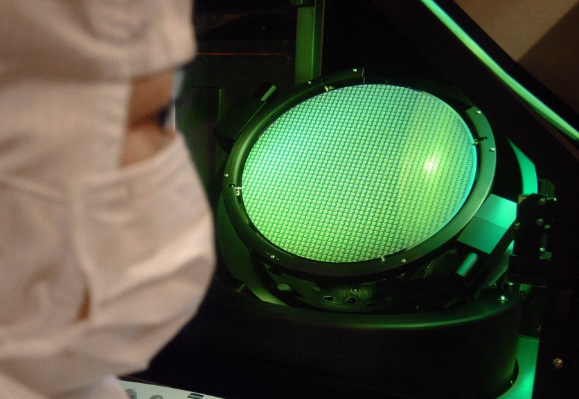
SAM YEH/Gettyimages.com
United Microelectronics Corporation reported its strongest quarterly performance in years on Tuesday, posting TWD 68.73 billion (approximately $2.12 billion USD; exchange rate as of July 29, 2026; conversions are approximate) in Q2 2026 revenue — a 12.6% sequential jump — while CEO Jason Wang confirmed for the first time that process design kits for the closely watched Intel 12nm FinFET node are on track to reach customers by the end of this year, according to the UMC Q2 2026 earnings call transcript. A reader who wants to understand whether UMC's five-year silicon photonics and advanced-node bet is paying off has that answer this morning: it is, and the timeline just got concrete.
The earnings beat — with gross margin expanding to 32.5% and factory utilization climbing to 85% from 79% a quarter earlier — arrived alongside a second major development: two weeks ago, on July 14, UMC and Singapore-based chip designer SILITH Technology announced the first delivery of mass-produced silicon photonics wafers from UMC's 12-inch fab in Singapore, putting a real customer's optical interconnect chips into production and validating UMC's claim that it can manufacture photonic ICs at 12-inch wafer scale, per the official UMC-SILITH press release. Together, those two developments answer the core question that has hung over UMC's stock — which is up 124% year-to-date even after a 1.67% premarket decline to $17.07 — for the better part of two years: can this company actually deliver on the roadmap it promised, as the earnings call transcript confirms?
Intel 12nm Partnership Moves From Promise to Design Enablement
The cooperation between UMC and Intel announced in January 2024 is structured around a revenue-sharing arrangement in which UMC runs 12-nanometer FinFET production at Intel's Ocotillo Technology Fabrication site in Chandler, Arizona, using Fabs 12, 22, and 32. By leveraging Intel's existing equipment, UMC avoids the capital cost of building a US fab from scratch — a tradeoff that analysts have noted makes the economics of the deal work without the $10–20 billion headline expense of a standalone facility.
What makes that structure relevant today is what Wang disclosed on the earnings call: process design kits are on track for delivery to customers by late 2026, and the first customer tape-outs — where a chip designer submits a finished design to the foundry for manufacturing — are expected to begin in 2027, with volume production anticipated in 2028.
A process design kit is the technical bridge between a foundry and its customers. It packages the manufacturing facility's design rules, transistor models, and layout constraints into a software-compatible format that chip designers use in tools from Cadence and Synopsys. Without a PDK, no customer can begin designing a chip for a given node. The PDK delivery schedule — late 2026 — is therefore the real gating milestone for the 2027 tape-out and 2028 volume forecasts: it starts the customer design clock, as discussed in broader semiconductor industry context with Intel's 18A in recent TechTimes coverage of quantum chip design enablement.
The 12nm FinFET node itself is technically well understood. A FinFET wraps its gate electrode around a thin vertical silicon "fin" on two or three sides — a 3D structure that replaced the flat planar transistors that powered chips from the 1960s through the early 2010s. At 12nm, this architecture delivers roughly 55% higher speed and twice the transistor density of a 28nm planar design, while consuming significantly less power — improvements that matter for the wireless, IoT, and connectivity chips UMC is targeting with this node.
Wang said on the call that the 12nm deal would be accretive to UMC's existing margins once volumes ramp, with 2027 functioning as a pilot phase and more meaningful revenue contributions arriving in 2028. He was measured on the question of whether UMC intends to push to nodes smaller than 12nm. "We have to first deliver the 12," Wang said. "We have to prove the business model as well." Industry reports have suggested Intel and UMC may be exploring a 3nm extension of the partnership, though neither company has confirmed it.
One structural detail the earnings call did not address is that the margin accretion from the Intel arrangement depends not just on UMC's manufacturing execution but also on the utilization levels of Intel's Arizona fabs, which are Intel Foundry's own assets running UMC's process flows under a revenue-sharing structure. An investor modeling UMC's 2028 margin profile from the 12nm deal is therefore also implicitly modeling Intel Foundry's health — a dependency that does not exist in a standard foundry customer relationship. As of this quarter, Intel Foundry has been separately reported to have achieved 85% yield on its 18A process and is manufacturing commercial products using High-NA EUV lithography, as reported by TechTimes on July 15, which supports the view that the Arizona facilities are technically capable partners.
Read more: Intel Foundry Breaks Customer Silence With Fortinet Deal as Q2 Earnings Approach
Silicon Photonics Crosses From Lab to Production Line
The July 14 SILITH announcement independently confirms what Wang described on Tuesday as one of UMC's most significant recent milestones: UMC delivered its first batch of mass-produced photonic integrated circuit wafers from its Singapore Fab 12i, using a 12-inch silicon-on-insulator process based on the imec iSiPP300 platform that UMC licensed in December 2025, as further detailed in TrendForce's coverage of the milestone.
The wafers support SILITH's 1.6-terabit silicon photonics platform — a system that moves 1.6 trillion bits of data per second down a fiber by encoding it as modulated light rather than electrical current, per the official UMC-SILITH press release. SILITH's end customers include optical transceiver manufacturers Innolight and Coherent, which are key optical suppliers to NVIDIA and Google — placing UMC's production directly in the AI data center supply chain, as TrendForce's analysis confirms.
The technical architecture involved is worth explaining for readers trying to evaluate UMC's claims against its competitors. The current platform uses silicon Mach-Zehnder Modulators — a component that splits a light beam into two paths inside a silicon waveguide, modulates the phase of each path electrically, then recombines them to encode data through interference, as analyzed in detailed semiconductor coverage. The 12-inch wafer format — as opposed to the 8-inch platforms operated by some rivals — means more chips per production run, lower per-unit cost, and the manufacturing scale that hyperscale customers require when placing large orders.
UMC and SILITH are extending that roadmap toward 400 gigabits per lane — a doubling of current per-lane bandwidth — using a pure-silicon MZM platform that preserves CMOS compatibility and avoids the cost and complexity of exotic materials, as confirmed in the joint press release. Separately, UMC is working with ecosystem partners on thin-film lithium niobate modulators for future ultra-high-bandwidth applications. TFLN offers wider electro-optic bandwidth than silicon alone, making it the leading candidate for 400G-per-lane and beyond — but this work is at the development stage, not in volume production.
UMC plans to open its 12-inch silicon photonics platform to general customer development in 2027 and aims to introduce an open platform by 2028, per TrendForce. The Singapore P4 facility is planned to receive a new clean room expansion to scale silicon photonics manufacturing capacity beyond the current SILITH relationship.
Why does this matter for co-packaged optics — the technology that AI data center architects increasingly treat as mandatory infrastructure? Co-packaged optics places optical transceivers directly alongside switch ASICs on the same substrate, eliminating the copper trace that connects separate pluggable modules to the chip. That copper trace becomes a power consumption and bandwidth bottleneck at the speeds AI clusters now demand; one analyst cited by Network World estimates CPO can reduce interconnect power by 60–70% compared to pluggable optical modules. UMC's 12-inch silicon photonics production positions it as a supply chain component for CPO systems targeting 3.2 terabit switching — the generation hyperscalers expect to need by 2027–2028.
Read more: Tower Semiconductor Commits $3 Billion to Silicon Photonics: Japan Backs the Bet
By the Numbers: A Quarter That Rewrites the Utilization Story
Second-quarter revenue of TWD 68.73 billion (approximately $2.12 billion USD) arrived at the top end of guidance, with gross margin expanding to 32.5% from 29.2% the prior quarter — a 330-basis-point improvement driven by the jump in factory utilization and a better product mix, per the earnings call transcript. Net income attributable to shareholders reached TWD 42.26 billion (approximately $1.30 billion USD), representing a 161% sequential increase and what Investing.com described as a near-quintupling from the year-ago period, as reported in the Q2 slides summary. Wafer shipments totaled 1.13 million 12-inch equivalent wafers — a 10.6% sequential increase, per the earnings call transcript.
For the first half of 2026, UMC posted revenue of TWD 129.77 billion (approximately $4.00 billion USD), net income of TWD 58.4 billion (approximately $1.80 billion USD), and earnings per ordinary share of TWD 4.68 (approximately $0.14 USD), per the earnings call. First-half gross margin of 30.9% ran approximately 300 basis points above the same period a year ago.
The company ended Q2 with cash on hand of approximately TWD 124.7 billion (approximately $3.84 billion USD) and total equity of TWD 443.9 billion (approximately $13.67 billion USD), per the earnings call transcript.
Wafer Prices Going Up: What Chip Designers and End Consumers Face
For anyone who designs, sources, or buys electronics, the pricing section of Tuesday's call carries direct implications. UMC notified customers in April 2026 of wafer price increases taking effect in the second half of the year — with some reports suggesting a roughly 10% hike beginning in July — and CFO Chih-Tung Liu confirmed on the call that the trend is constructive and accelerating, with more substantial negotiations expected in 2027, per TrendForce's coverage and the earnings call transcript.
The customers absorbing those increases span MediaTek, Qualcomm, Broadcom, Texas Instruments, Realtek, and hundreds of smaller chip companies; reporting by WCCFTech, citing the April customer letter, described the situation as one where customers have "no alternative" given tight global foundry capacity, as documented in WCCFTech's coverage of the wafer price increase. The cost typically passes through to electronics OEMs and, ultimately, to consumer product prices, though how much and on what timeline varies by category.
UMC's pricing power is partly a function of dynamics outside its direct control. Chinese foundry SMIC — the state-backed manufacturer that posed a serious pricing threat after cutting 28nm wafer prices by roughly 40% in early 2025, dropping from approximately $2,500 to $1,500 per wafer — has since reversed course with its own price increases as domestic Chinese utilization exceeded 95%, per Tom's Hardware's trailing-edge foundry analysis. After two years of price pressure driven by Chinese capacity expansion, the mature-node segment appears to have found a floor, and UMC is capturing the recovery.
Q3 Outlook: Above 90% Utilization, Margins in the Mid-30s
Wang guided Q3 2026 wafer shipments higher by a high-single-digit percentage sequentially — implying total volumes above 1.2 million 12-inch equivalent wafers — with gross margin expected in the mid-30% range and overall factory utilization projected to exceed 90%, with 12-inch capacity already running above the corporate average and 8-inch expected to reach the mid-80% range, per the earnings call transcript.
Wang attributed the demand momentum to power management ICs, sensors, and microcontrollers — AI-adjacent categories that feed the data center infrastructure buildout at the mature-node layer rather than the leading edge. Consumer electronics, including handsets, PCs, and notebooks, remain soft, he acknowledged. The recovery is broad enough that it is not dependent on a single end market.
Capital Expansion: $2 Billion This Year, $5 Billion Through 2027
UMC's board approved raising 2026 capital expenditure to $2 billion USD, with a total board-approved plan of approximately $5 billion USD across 2026 and 2027, allocated 90% toward 12-inch wafer capacity in silicon photonics and advanced packaging, per the Q2 slides. This expansion covers two projects:
At Singapore's P4 facility, a new clean room will expand silicon photonics manufacturing capacity, building on the SILITH mass-production milestone and supporting the planned 2027 general availability of UMC's silicon photonics platform for new customers.
At UMC's 12A campus in Tainan, Taiwan, phases P7 and P8 will construct a new facility focused on advanced packaging — specifically logic-and-memory stacking and what management calls "discrete through-chip connections" (DTC), a form of chiplet interconnect technology that enables tight integration of different chip types without requiring them to be manufactured on the same process node, per the earnings call. Wang noted that UMC currently works with more than 10 active advanced packaging customers, with over 35 new products in discussion for tape-out in 2026 and early 2027.
Construction lead times of approximately 20 months mean neither facility will begin ramping capacity until 2028 or early 2029. CFO Liu told analysts that depreciation is expected to rise by low-teens percentages annually for at least the next two years as these facilities come online — guidance that likely weighed on the premarket stock reaction despite the results themselves being strong.
How Is UMC Positioned Against the Competition?
UMC's strategic position in the mature-node segment has become more complicated in the past 18 months, as SMIC's market capitalization has reportedly grown to roughly three times UMC's on the back of state investment and domestic Chinese demand — and, by some measures, SMIC has overtaken UMC in global foundry revenue, as SmBom's competitive analysis documents. SMIC remains constrained by US export controls that limit its access to EUV lithography tools and cap its yield on advanced nodes; its 7nm capacity operates at yields estimated at 20–40% by some analysts, making it uncompetitive outside a protected domestic market.
UMC's response to that competitive pressure is not to match SMIC's pricing at commodity nodes — it is to move up the value stack through specialty processes, silicon photonics, and advanced packaging where Chinese foundries cannot easily follow. The Intel 12nm cooperation extends that logic to FinFET territory: UMC gains access to a more advanced node without the full capital burden of building the manufacturing capability from scratch, while offering customers US-manufactured supply chain optionality that SMIC cannot provide.
Whether the bet pays off in margins and returns depends heavily on execution over the next 24 to 36 months. Tuesday's results suggest the execution track record is improving.
How UMC Stock Reacted — and What the Analysts Said
UMC's U.S.-listed American depositary receipts fell 1.67% in premarket trading on Tuesday, declining to $17.07 from the prior session's close of $17.36, per the earnings call transcript. The stock has had a volatile recent stretch — down approximately 18.5% over the prior week — even as its year-to-date gain of 124% remains remarkable. The premarket decline likely reflects a familiar tension in foundry investing: rising depreciation and multi-year capital commitments weigh on near-term free cash flow even when operating performance is strong.
Wedbush Securities analyst Matt Bryson maintained a Neutral rating with an NT$80 price target, highlighting before the results that the revenue outperformance — secured even before the new pricing adjustments took full effect — demonstrates "authentic momentum" in UMC's core operations. Citi analyst Laura Chen and Morgan Stanley analyst Charlie Chan both pressed management on the pricing and AI demand outlook during the call, per the earnings call transcript. Bernstein maintained an Underperform rating with a $7.40 target, representing a more skeptical view on whether the capex cycle produces adequate returns, as Blockonomi's post-earnings analyst roundup documents.
The split between Wedbush's Neutral and Bernstein's Underperform captures the live investor debate: the operating trends are clearly improving, but the margin durability — given rising depreciation — is the question.
Frequently Asked Questions
When will Intel 12nm chips from the UMC-Intel cooperation reach volume production?
Process design kits are targeted for delivery to chip designers by late 2026, which starts the customer design process. Customer tape-outs — where completed chip designs are submitted to the fab — are expected to begin in 2027, with volume production meaningful enough to register in UMC's financial results anticipated in 2028. The 2028 timeline is management's projection; it depends on PDK delivery, customer design cycle timing, and Intel's Arizona fab utilization levels.
What is UMC's 12-inch silicon photonics platform, and why does it matter for AI?
UMC delivered its first mass-produced silicon photonic integrated circuit wafers on July 14, 2026, to SILITH Technology, whose optical interconnect chips supply manufacturers serving NVIDIA and Google. The platform uses silicon Mach-Zehnder Modulators on a 300mm silicon-on-insulator wafer format, moving more data per production run at lower cost than 200mm alternatives. This positions UMC as a supply chain component for co-packaged optics — the technology that replaces copper traces with optical links inside data center switches, reducing interconnect power consumption by an estimated 60–70% at the speeds AI workloads require.
How much are UMC's wafer prices increasing, and who pays?
UMC formally notified customers in April 2026 of wafer price increases taking effect in H2 2026, with industry reports suggesting approximately 10% starting in July. CFO Chih-Tung Liu indicated that pricing negotiations with customers will intensify further in 2027. The increase affects major chip companies — MediaTek, Qualcomm, Broadcom, Texas Instruments, and many others — who typically pass costs downstream to electronics OEMs, and ultimately to consumer products, though the degree and timing vary by product category.
Why did UMC stock fall even though the quarter beat expectations?
The market reaction reflects concern about what follows a strong quarter, not the quarter itself. UMC's board approved $2 billion in capital expenditure for 2026 and approximately $5 billion total through 2027, with depreciation expected to rise by low-teens percentages annually for at least two years. Investors are weighing whether the revenues from silicon photonics, advanced packaging, and the Intel 12nm ramp will materialize in time to offset that cost headwind — and Bernstein's Underperform rating suggests not everyone is convinced.

-
 C114 Communication Network
 -
 Communication Home
