
 Search

Intel.com
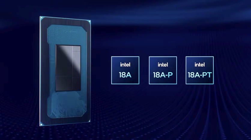
The most consequential deliverable in Hitachi's new quantum computing roadmap is not a qubit count — it is a design kit. When Hitachi announced on July 22 that Japan's government had selected it to lead a quantum computing initiative built around Intel's 18A semiconductor process, the headline milestone that followed in most coverage was the 1,000-qubit target for fiscal 2030. The milestone that will matter more to the next decade of quantum hardware development is what Hitachi and Intel plan to produce alongside it: a process design kit for silicon spin-qubit chips on one of the world's most advanced semiconductor nodes — the first tool of its kind for a 1.8nm-class process, and the key that would allow any engineering team on earth to design quantum chips for industrial fabrication without rebuilding from scratch the process knowledge that Hitachi and Intel will encode in it.
The project, formalized under Japan's New Energy and Industrial Technology Development Organization as part of the "Accelerating the Development and Demonstration of Next-Generation Quantum Computers to Solve Social Challenges" program, pairs Hitachi with Intel's Japanese subsidiary, Intel K.K., and the National Institute of Advanced Industrial Science and Technology (AIST). It runs through March 2029 and expands a broader strategic collaboration the two companies first announced on June 5, 2026.
Why a Quantum PDK on Intel 18A Is the Project's Most Significant Deliverable
In classical chip design, process design kits are what make semiconductor development accessible at scale. A PDK packages a fab's manufacturing rules, device models, and layout constraints so that circuit designers can build chips using standard electronic design automation software — Cadence, Synopsys — without negotiating each design decision with process engineers. When SkyWater Technology made its 130nm PDK open-source in 2020, it enabled university research groups and small companies to tape out real silicon on a commercial foundry without requiring proprietary fab relationships. That democratization produced a wave of academic chip projects that would have been financially impossible the year before.
No equivalent tool currently exists for silicon spin-qubit chips on an advanced semiconductor node. What the Hitachi-Intel project will produce — a quantum PDK on Intel 18A — would be the first such interface for a 1.8nm-class process: a common design language that allows any team to design silicon spin-qubit hardware for industrial fabrication, inheriting the process maturity that Hitachi and Intel encode in the kit rather than having to replicate it from scratch.
That is why AIST G-QuAT Deputy Director Masahiro Horibe described the initiative as designed to "accelerate the formation and expansion of the ecosystem." Ecosystem formation in semiconductors does not happen through adding headcount at incumbent organizations — it happens when external engineers gain a standardized design interface.
Four Technical Pillars Targeting Scale
The project is organized around four parallel workstreams. Hitachi and Intel K.K. will co-develop chip architectures targeting 100 or more qubits, engineered to meet the manufacturing consistency expected from semiconductor production lines — meaning performance must be controllable across wafers, not only demonstrated in a single laboratory device. This workstream will also develop cryogenic packaging and peripheral control circuits capable of operating at the millikelvin temperatures silicon spin qubits require.
The second workstream builds the silicon quantum PDK on Intel 18A. The third addresses the wiring bottleneck: as qubit counts grow, routing individual control and readout connections from room-temperature electronics into the dilution refrigerator's millikelvin stage consumes its limited cooling budget — approximately 30 microwatts at the coldest stage — long before a meaningful qubit array can be assembled. Hitachi will develop high-density 3D integration technologies — stacking qubit chips and control electronics vertically — designed to operate at cryogenic temperatures with short, dense interconnects that sidestep the long wire runs that make current architectures thermally infeasible at scale.
The fourth workstream, led by AIST, will operate an open cloud computing platform through AIST's Global Research and Development Center for Business by Quantum-AI Technology (G-QuAT) facility, developed at a cost of approximately ¥62 billion (approximately $379 million USD). Exchange rate as of July 28, 2026; conversions are approximate. That platform already hosts Japan's first commercial optical quantum computer — OptQC's MoQuren system, deployed as part of the ABCI-Q hybrid infrastructure. The new cloud access will extend that infrastructure to silicon spin-qubit hardware, making experimental quantum hardware accessible to outside researchers without requiring them to own a dilution refrigerator.
How Silicon Spin Qubits Work — and Why Intel 18A
A silicon spin qubit stores one unit of quantum information in the spin state of a single electron trapped inside a nanoscale region of silicon called a quantum dot — a structure roughly 50 nanometers (about 0.002 inches) across, defined by voltage-controlled gate electrodes patterned in the silicon. The electron can be spin-up, spin-down, or a quantum superposition of both simultaneously. Logic operations are performed by applying microwave pulses at the electron's resonant frequency; two-qubit gates exploit the exchange interaction between electrons in adjacent quantum dots.
The reason CMOS manufacturing compatibility matters here is cost and scalability. Unlike superconducting qubits — which require niobium-based deposition equipment and bespoke cryogenic packaging not found in commercial chip factories — silicon quantum dots can be fabricated using the same extreme-ultraviolet lithography, ion implantation, and gate-stack deposition processes that run on mainstream 300mm production lines. Silicon spin qubits are also approximately 1,000 times smaller than the superconducting transmons used in IBM and Google systems, which means far more can fit on a chip of identical size. And while superconducting qubits require cooling to roughly 15 millikelvin (approximately −459.66°F/−273.14°C), silicon spin qubit demonstrations have run at 1 Kelvin (approximately −457.87°F/−272.15°C) — still colder than outer space, but far less demanding on refrigeration infrastructure.
Intel 18A, which entered high-volume production at Fab 52 in Chandler, Arizona in late 2025 for Panther Lake laptop processors and Clearwater Forest server chips, introduced two architectural advances simultaneously. RibbonFET is Intel's implementation of gate-all-around transistor architecture, in which the gate electrode wraps the silicon nanosheet channel on all four sides — delivering tighter electrostatic control than prior FinFET designs and reducing device-to-device variation. PowerVia moves the power delivery network to the backside of the wafer, freeing front-side routing layers for signal connections. Both properties transfer directly to quantum chip manufacturing: RibbonFET's reduced variation improves quantum dot uniformity, and PowerVia's freed routing layers create space for the dense gate arrays needed to address individual qubits.
Intel's in-house silicon quantum hardware program has been building toward this manufacturing capability for years. The company developed Horse Ridge, a cryogenic control ASIC that operates at 4 Kelvin (approximately −452.47°F/−269.15°C) to manage qubit manipulation and readout from inside the cryostat. Its 12-qubit Tunnel Falls test processor began shipping to research collaborators including Argonne National Laboratory in early 2026. Intel has separately been developing Pando Tree, a next-generation cryogenic control program that aims to place control electronics at the millikelvin stage itself — co-located with the qubits — which would reduce the cabling complexity that presently limits all silicon spin qubit systems. Single-qubit gate fidelities above 99.7% have been demonstrated in academic collaborations using Intel's silicon spin platform.
What These Milestones Are — and Are Not
The 100-qubit target for FY2028 and the 1,000-qubit target for FY2030 need to be understood in context. They are research-scale engineering prototypes, not fault-tolerant quantum computers.
Fault-tolerant quantum computing — the regime where a machine corrects its own errors reliably and can execute the deep circuits needed to break RSA-2048 encryption or run large-scale molecular simulation — is generally expected to require on the order of one million physical qubits, once the overhead of quantum error correction is factored in. Surface code error correction, the most widely studied approach, requires hundreds to more than a thousand physical qubits to encode a single error-free logical qubit. A system that reaches 1,000 physical qubits might therefore support tens of logical qubits — enough for research algorithms, but nowhere near the threshold for practical fault-tolerant applications.
Silicon spin qubits also lag competing technologies in raw qubit counts today. Fujitsu and RIKEN's parallel NEDO-backed program — using superconducting qubits rather than silicon — deployed a 256-qubit system in April 2025 and has been targeting 1,000 qubits in fiscal 2026. IBM's superconducting roadmap and Quantinuum's trapped-ion systems are operating on similar or more aggressive timescales.
The wiring bottleneck that Hitachi's 3D packaging work targets has also not yet been demonstrated at the qubit counts the project is aiming for. Maud Vinet, CEO of Quobly — a CEA-Leti and CNRS spinoff that is itself fabricating silicon spin qubits on STMicroelectronics' commercial FD-SOI manufacturing line — observed in 2025 that current silicon spin qubit prototypes rely on wiring that is not scalable beyond dozens of qubits, and that cryogenic CMOS integration is essential for both reducing wiring complexity and minimizing latency in quantum error correction.
What the project aims to deliver is not fault tolerance but the manufacturing foundation that would make the longer journey possible: qubit chip designs that a commercial fab can reproduce consistently, a PDK that opens that capability to the wider community, and a cloud platform that gives researchers their first empirical window into how Intel 18A performs as a platform for quantum chip fabrication.
Intel 18A's Foundry Competitive Dimension
Beyond its quantum significance, the Hitachi partnership carries weight for Intel's foundry business. Intel 18A has been central to Intel CEO Lip-Bu Tan's foundry turnaround narrative — Panther Lake is already in production at Fab 52 in Chandler, Arizona, and a Clearwater Forest server variant is also shipping on the same node. Converting internal production success into external customer commitments has proven harder than demonstrating the process's technical capability.
In May 2026, Tan confirmed publicly that Intel's foundry business had "multiple customers engaged" and that improvements in its 18A and 14A processes were driving increased interest from potential customers — citing deals already signed with Tesla and Google. The Hitachi collaboration makes Hitachi the first publicly confirmed Japanese customer using the 18A process for external foundry work, a significant symbolic and commercial milestone as Intel works to build an ecosystem around the node ahead of its 14A roadmap.
The timing is also notable because, on the same day Hitachi's NEDO announcement landed, IBM announced a definitive agreement to acquire HRL Laboratories — the Boeing and General Motors joint research institution that had built the world's most advanced published silicon spin-qubit processor, an 18-qubit device with 54 quantum dots demonstrated in April 2026. IBM intends to route HRL's silicon spin expertise through its Anderon quantum wafer foundry in Albany, New York — a separate manufacturing path from Intel 18A. The competitive consolidation of July 22–23, 2026 placed IBM and the Hitachi-Intel-AIST consortium in parallel races to own the manufacturing standard for silicon spin quantum chips at industrial scale.
Japan's Larger Quantum Strategy
The project fits within a national quantum program Japan has been building since 2022. The Cabinet Office's Quantum Future Society Vision and Quantum Future Industry Strategy designated quantum computing, communications, and sensing as national priorities. Japan's Moonshot Research and Development Program, Goal 6, targets a fault-tolerant universal quantum computer by 2050. Government funding across national quantum programs through MEXT, NEDO, and JST has exceeded ¥150 billion (approximately $916 million USD) committed across the national strategy period.
Hitachi's own quantum research history runs deep. The company has been developing silicon quantum-dot qubits since the early 2000s and holds 15 patent families in the silicon spin-qubit space. It has participated in Japan's Moonshot Program and collaborated with imec, the Belgian semiconductor research institute that demonstrated full-wafer EUV-patterned silicon spin qubits at IEDM 2025, as confirmed in imec's SPINS program documentation. It is also a member of Q-STAR, the Quantum Strategic Industry Alliance for Revolution, whose membership includes Toyota, NEC, Fujitsu, NTT, and more than 100 other corporate members.
AIST's G-QuAT facility, developed at a cost of approximately ¥62 billion (approximately $379 million USD), has become the hub for this national strategy's hardware. It hosted Japan's first commercial optical quantum computer — OptQC's MoQuren system, deployed as part of the ABCI-Q hybrid infrastructure — before the Hitachi-Intel silicon spin project was added to its portfolio. The addition of silicon spin hardware on Intel 18A makes AIST G-QuAT one of a small number of sites globally where multiple distinct qubit architectures can be accessed through a single research cloud platform.
Hitachi CTO Shigetoshi Samejima described the project in terms that connect quantum computing to the company's Lumada digital services strategy: "Hitachi positions quantum computers as a strategic technology that can break through the limits of computation itself and support future social infrastructure and industrial systems." Intel K.K. President Makoto Ohno framed the collaboration's purpose around the manufacturing transition: the initiative is designed to establish "foundational chip design, manufacturing and packaging technologies needed to move silicon quantum computing from research demonstration toward scalable industrial application," according to The Quantum Insider.
The cloud service planned for FY2027 will be the first external test of whether that transition is underway, offering researchers their initial window into how Intel 18A performs as a platform for quantum chip fabrication — and whether a commercial semiconductor foundry can become a quantum hardware factory on the timeline Japan, Intel, and Hitachi are betting it will.
Frequently Asked Questions
How do silicon spin qubits work, and why does manufacturing compatibility with CMOS fabs matter?
A silicon spin qubit stores quantum information in the spin state of a single electron trapped in a quantum dot — a nanoscale region of silicon defined by voltage-controlled gate electrodes. The electron can be spin-up, spin-down, or a quantum superposition of both simultaneously. Logic gates are performed using microwave pulses and the exchange interaction between adjacent electrons. The reason fab compatibility matters is that the lithography equipment, materials, and process flows needed to build silicon quantum dots already exist at scale in commercial 300mm chip factories. No other major qubit technology shares this manufacturing heritage — superconducting qubits require niobium deposition equipment not found on commercial lines, and trapped-ion systems require entirely different fabrication infrastructure. Silicon spin qubits are the only qubit type that could, in principle, scale using existing industrial capacity rather than requiring entirely new production facilities.
What is a process design kit, and why does an Intel 18A quantum PDK matter?
A process design kit (PDK) is a collection of manufacturing rules, device models, and layout constraints that allows chip designers to build circuits compatible with a specific fab's production process using standard electronic design automation software. Without a PDK, designing a chip for a fab requires case-by-case negotiation with process engineers. When SkyWater released its 130nm PDK in 2020, it enabled university research groups and small companies worldwide to design and fabricate real silicon without requiring proprietary fab relationships — transforming chip design from a gated activity into an open engineering discipline. A silicon quantum PDK on Intel 18A would do the same for quantum chip design: any engineering team with standard EDA tools could design silicon spin-qubit hardware for industrial fabrication, inheriting the process maturity that Hitachi and Intel encode in the kit. No equivalent tool currently exists for an advanced-node quantum process.
How does this project's roadmap compare to other silicon spin qubit efforts globally?
Several parallel efforts are working toward the same goal of industrial silicon spin qubit manufacturing. IBM's announced acquisition of HRL Laboratories — a Boeing and General Motors research institution — on July 23, 2026 gives IBM access to silicon-spin qubit expertise it plans to route through its Anderon quantum wafer foundry in Albany, New York. In France, Quobly is fabricating silicon spin qubits on STMicroelectronics' commercial FD-SOI process line and plans to offer cloud access through OVHcloud in late 2026. In Belgium, imec launched its SPINS semiconductor spin-qubit pilot line in April 2026 with 25 partners on 300mm CMOS manufacturing lines. The distinguishing feature of the Hitachi-Intel-AIST project is its use of a 1.8nm-class advanced process node — Intel 18A — with a planned shared PDK deliverable, which positions it as an attempt to set a quantum manufacturing standard rather than build a proprietary internal capability.
When will any of this be available for researchers or enterprises to use?
Cloud-based access to experimental silicon quantum hardware via AIST's G-QuAT is targeted for fiscal 2027 — by March 2028 at the latest. That access will be for research and experimental workloads, not general-purpose computing. The 100-qubit prototype implementing quantum error-correcting codes is targeted for fiscal 2028. The 1,000-qubit platform is targeted for fiscal 2030. Fault-tolerant quantum computing — where machines reliably correct their own errors and can execute commercially useful algorithms — is expected to require on the order of one million physical qubits; none of the project's milestones reach that threshold. They represent intermediate engineering achievements on the manufacturing path toward it.

-
 C114 Communication Network
 -
 Communication Home
