
 Search

Ats.net
For years, the semiconductor industry's great anxiety was silicon: whether foundries could shrink transistors fast enough, manufacture wafers in sufficient volume, and keep pace with the exponential demands of artificial intelligence. That bottleneck, according to the CEO of one of the world's most strategically positioned chip substrate makers, has now moved — and it has moved to a layer of the supply chain that most AI infrastructure planners have not yet fully priced in.
"The bottleneck has shifted," Dr. Michael Mertin, CEO of AT&S Austria Technologie & Systemtechnik AG, told Nikkei Asia on Monday from Malaysia. "It's no longer chip fabrication. It's packaging."
AT&S — an Austrian manufacturer of integrated circuit (IC) substrates and high-end printed circuit boards listed on the Vienna Stock Exchange — sits at a critical but frequently overlooked junction of the AI supply chain. Its products are the physical foundation connecting chip dies together inside every advanced AI accelerator: the substrate, the interconnect film, the wiring beneath the processor. And right now, Mertin says, demand for those products is running well ahead of the industry's ability to supply them.
Read more: Global Chip Race Fractures Into Four Strategies: US Packaging Gap Remains After $265B Bet
How CoWoS Became the Last Step That Nothing Can Skip
To understand the bottleneck AT&S is describing, it helps to understand what advanced packaging actually does — and why it is now the mandatory gate every AI chip must pass through.
Modern AI accelerators are not monolithic silicon dies. Nvidia's Blackwell and Rubin chips, AMD's MI-series, and the custom ASICs built by Google, Amazon, and Meta are complex assemblies of multiple chiplets: a logic die handling computation, stacks of High Bandwidth Memory (HBM) for data throughput, and I/O components, all of which must be connected together with extraordinary precision. The technology that makes this connection possible is TSMC's Chip on Wafer on Substrate platform, abbreviated CoWoS (pronounced "cow-os").
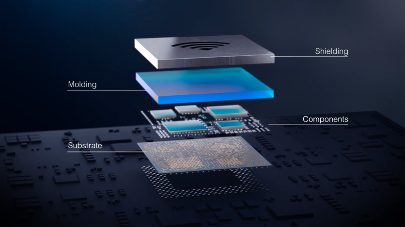
In a CoWoS package, the GPU logic die and HBM stacks sit side by side on a passive silicon bridge called an interposer, which TSMC describes in its CoWoS technology documentation as studded with microscopic copper-filled channels called through-silicon vias, enabling memory bandwidth in the terabytes-per-second range — data rates that conventional printed circuit board traces cannot approach and that modern large language models require to run. The assembled chip-and-memory unit is then mounted on an organic substrate — the layer AT&S manufactures — which connects the entire assembly to the server board below. Hence the name: chip on wafer on substrate.
Without CoWoS, a perfectly fabricated 3-nanometer wafer cannot become a functional AI chip. It is the last mandatory step in a long assembly line — and the one that is now sold out.
TSMC CEO C.C. Wei acknowledged the severity at the company's annual shareholder meeting in June, stating that CoWoS capacity remains "extremely tight and sold out through 2026." Lead times for CoWoS assembly are running 52 to 78 weeks, which means an AI chip designer submitting an order today cannot reasonably expect delivery before mid-2028 in many cases.
The scale of the ramp TSMC is attempting reflects how severe the gap is. The company is scaling CoWoS production from approximately 35,000 wafers per month in late 2024 to a projected 130,000 by year-end 2026 — a near four-fold increase in under two years. By the company's own projection, it still falls short. Demand for 2026 is estimated near one million wafers total; supply is running at roughly 80% of that figure.
Nvidia's Commanding Hold on Available Capacity
The reason supply cannot catch demand is, in large part, one company. Nvidia is estimated to hold roughly 60% of total global CoWoS capacity for 2026 — approximately 595,000 wafers — drawn from TSMC's lines and supplementary capacity at third-party packagers Amkor and ASE. The top three customers combined — Nvidia, Broadcom, and AMD — account for an estimated 85% or more of total capacity allocation. Smaller players building AI chips, from well-funded startups to hyperscaler ASIC teams at Amazon and Google, are left competing for the remainder.
The pricing signal confirms the scarcity. Advanced packaging prices are rising at two to four times the rate of the underlying wafers — an unusual inversion in a supply chain that has historically competed on die cost per unit.
ABF Film: Monopoly Risk Beneath the Packaging Crunch
The CoWoS capacity crunch and the shortage of substrate materials are related but structurally distinct problems — and the second is, in some ways, the more alarming of the two.
CoWoS capacity is constrained by a limited number of specialized facilities and the long lead times to build new ones. That is a capacity problem: given enough time and capital, it can be expanded. The substrate material shortage is something different. The critical insulating film used in every high-performance AI chip substrate — Ajinomoto Build-up Film, universally called ABF — is supplied by a single company, Ajinomoto Fine-Techno, which holds approximately 95% of the global market. Ajinomoto is a Japanese food and chemical conglomerate best known for producing monosodium glutamate. Its subsidiary controls the input material for the substrates inside every Nvidia GPU, every AMD Instinct accelerator, and every high-end networking ASIC on the market.
When AI chip packaging layers evolved from three-layer configurations to eleven-layer configurations — as the complexity of AI accelerators has demanded — total ABF consumption per chip multiplied dramatically, even without any increase in unit volume. The result is an ABF supply-demand gap that is widening faster than capacity can respond.
Ajinomoto notified substrate manufacturers in May 2026 that it would raise ABF film prices by approximately 30%, with new pricing taking effect in the third quarter of 2026. The price hike — combined with similar increases on copper-clad laminate materials from Japan's Resonac and Mitsubishi Gas Chemical — is placing broad-based cost pressure on the entire IC substrate supply chain. For substrate manufacturers, a 30% increase in ABF film cost translates to a 3% to 6% increase in finished substrate prices.
Industry projections place the ABF supply-demand gap at approximately 10% in the second half of 2026, widening to around 21% in 2027, and potentially exceeding 40% by 2028, as AI chip generations continue to grow in size and layer count. Lead times for finished ABF substrates are running 16 to 24 weeks and are expected to remain there through 2027. Samsung Electro-Mechanics has announced a $1.2 billion investment to expand its own ABF substrate manufacturing lines, with volume production not expected until the third quarter of 2027.
Ajinomoto itself is planning a third ABF production facility in Gifu Prefecture, Japan — an investment of ¥1.2 billion (approximately $7.3 million) in land acquisition, with the plant targeted for completion in 2032. Even at that pace, analysts project the supply gap widening before it narrows.
Exchange rates as of July 26–27, 2026; conversions are approximate.
Taiwan's three dominant substrate fabricators — Unimicron, Kinsus Interconnect, and Nan Ya PCB — are operating at full capacity utilization and are expected to remain there through year-end.
AT&S and the Co-Development Shift
Against this supply-constrained backdrop, AT&S has made a $2.85 billion bet (more than €2.5 billion, exchange rate as above) on becoming the preferred substrate partner for the AI era — and its share price reflects a market that believes the strategy is working.
The company's shares were trading near €13 (approximately $15) in early 2025, when Mertin took over as CEO, inheriting a company that had struggled through a painful expansion cycle under his predecessor. By June 2026, after announcing a €1.5 to €2 billion (approximately $1.71 to $2.28 billion) expansion of its Kulim, Malaysia manufacturing site, the stock hit a record high of approximately €200 (approximately $228) per share, pushing the company's market capitalization to around €7.58 billion (approximately $8.64 billion). The expansion is supported by long-term supply commitments from AMD and a second technology company that AT&S has not named publicly, though industry sources identify the second customer as Intel. AT&S reported consolidated revenue of €1.8 billion (approximately $2.05 billion) for its 2025–2026 fiscal year, up 21% on a currency-adjusted basis.
The company is aiming to have at least five major US technology companies as customers as its Kulim capacity comes online, and is simultaneously expanding its Chongqing, China facility to serve a separate customer base in mobile and consumer segments.
Beyond the physical supply crunch, Mertin argues the AI boom has forced a structural change in the relationship between chip designers and packaging suppliers that the industry has not yet fully adapted to.
"You have to cooperate, you have to think, you have to have a joint roadmap," he told Nikkei Asia. In traditional semiconductor supply chains, packaging suppliers were largely commodity vendors: they received specifications, manufactured to order, and competed primarily on cost and yield. That model, Mertin argues, no longer works.
The reason is complexity. As AI accelerators integrate more chiplets on a single substrate — stacking memory, logic, and I/O in increasingly dense 2.5D and 3D configurations — the communication density and power delivery demands on the substrate itself become a primary design constraint. The substrate is no longer a passive carrier; it is an active element of the chip's architecture. Substrate suppliers like AT&S must now be involved in the design process from the earliest stages, co-developing material specifications, layer counts, and interconnect geometries alongside the chip designers. Mertin previously compared the complexity of IC substrates to wiring an 80-story skyscraper — then multiplying that complexity millions of times and compressing it into a tiny flat device.
This shift has significant competitive implications. Packaging suppliers capable of forming co-development partnerships — and maintaining confidential joint roadmaps with customers — will be structurally favored over arm's-length manufacturers. It also raises barriers to entry, as new capacity entrants must offer not just manufacturing scale but engineering intimacy.
Read more: TSMC Posts Record Quarter as AI Chip Demand Pushes Full-Year Growth Outlook Past 40%
Why This Shortage Cannot Be Fixed by Ordering More Chips
The broader supply chain picture reinforces Mertin's warning. Through the first quarter of 2026, supply constraints spread beyond semiconductors into specialty gases, power components, advanced optics, and thermal infrastructure simultaneously, with multiple supply chain categories entering active shortage concurrently at lead times ranging from 20 to over 128 weeks for the most constrained items.
Critically, analysts and industry executives argue this shortage differs structurally from the semiconductor oversupply cycle that followed the 2021–2022 pandemic crunch. That episode was corrected through inventory drawdown — excess chips worked their way through the supply chain until demand and supply rebalanced. The current shortages cannot be resolved the same way, because the constrained materials — ABF film, specialty fiberglass cloth, advanced substrates — are consumed in production with no channel inventory accumulating. Meanwhile, hyperscaler demand is capital-committed at multi-year horizons, with no consumer demand normalization on the horizon to dampen the signal.
Supply correction requires new capacity — and new capacity in ABF film, IC substrates, and CoWoS packaging infrastructure takes two to four years to build from commitment to volume production.
That timeline is the crux of Mertin's warning. The world's AI infrastructure buildout — the data centers, the training clusters, and the inference servers absorbing hundreds of billions of dollars in capital expenditure from Microsoft, Google, Amazon, Meta, and their competitors — depends on a supply chain layer that takes years to expand, is controlled by a handful of highly specialized manufacturers, and is already running at its limits.
The chips are being fabricated. The packaging and substrates to complete them often are not.
Frequently Asked Questions
What is CoWoS and why is it creating a bottleneck for AI chips?
CoWoS — Chip on Wafer on Substrate — is TSMC's advanced packaging technology that physically connects AI processors and high-bandwidth memory stacks into a single, high-performance unit. Without it, a fabricated AI chip die is not a shippable product. The bottleneck exists because CoWoS requires specialized equipment, facilities, and processes that take years to build, and demand from AI chip designers — led by Nvidia, which holds roughly 60% of available CoWoS capacity — is outpacing the most aggressive capacity expansion TSMC has ever undertaken, according to the Silicon Analysts allocation tracker.
What is ABF film, who makes it, and why does one company control almost all of it?
Ajinomoto Build-up Film (ABF) is the insulating layer inside the organic substrate that connects a packaged AI chip to its circuit board. It enables the fine-line copper routing that modern chips require, making it irreplaceable in current chip substrate manufacturing. Ajinomoto Fine-Techno, the electronic materials subsidiary of the Japanese food conglomerate best known for MSG, developed the material in the 1990s and first commercialized it in 1999 — and holds approximately 95% of the global market, because the film requires highly specialized chemical expertise that no rival has been able to replicate at competitive scale.
How long are current lead times for advanced chip packaging, and what does that mean for AI infrastructure plans?
CoWoS assembly lead times are running 52 to 78 weeks — roughly one to one and a half years from order to delivery — for most customers not named Nvidia. ABF substrates carry additional lead times of 16 to 24 weeks. An enterprise or cloud provider planning AI infrastructure today should assume the packaging and substrate supply chain adds at least one to two years to delivery timelines, on top of any silicon fabrication lead time, making supply commitments made now critical to infrastructure deployments planned for 2027 and 2028.
What is AT&S, and why is an Austrian company at the center of AI chip manufacturing?
AT&S Austria Technologie & Systemtechnik AG is an Austrian manufacturer of IC substrates and high-end printed circuit boards — headquartered in Leoben, Austria, with major production facilities in Kulim, Malaysia; Chongqing, China; and Leoben. It is one of the few companies in the world capable of producing the advanced IC substrates required for AI-class chips at high volume. Its position in the supply chain — making the physical substrate that sits between the chip assembly and the server board — is obscure by consumer standards but strategically critical: without qualified substrate suppliers like AT&S, chip designers cannot convert fabricated silicon into shippable AI accelerators.

-
 C114 Communication Network
 -
 Communication Home
