
 Search

Nvidia.com
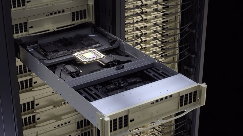
The board is roughly the size of a kitchen table. Three separate 26-layer circuit boards, each carrying copper traces no wider than one quarter of a human hair, are laminated together under heat and pressure into a single 78-layer stack. Every GPU-to-GPU signal inside Nvidia's planned Kyber NVL144 rack — 144 of its most powerful Rubin Ultra AI accelerators operating as a single unified compute domain — would pass through that board. On Monday, July 6, semiconductor research firm SemiAnalysis reported that Nvidia cannot yet build it at production volumes. The next-generation Kyber rack has been pushed more than 12 months past its 2027 target, to sometime in 2028.
Nvidia's response: "Our roadmap is intact."
That four-word answer is where the story currently sits — a terse denial on one side, and on the other, a detailed technical account from the firm that Jensen Huang mentioned by name at GTC in March, describing a manufacturing failure at the absolute physical frontier of what printed circuit board fabrication can currently achieve.
Read more: NVIDIA Vera Rubin Ships This Fall: 8 Cloud Partners, 10x Lower Token Cost, HBM4 Triples Bandwidth
Kyber's Orthogonal Backplane: Why This Board Matters
To understand what failed, it helps to know what Kyber was supposed to replace. The current Nvidia NVL72 rack — the one that went into full production in June and is now scheduled for delivery to eight cloud partners this fall — uses approximately 5,000 copper cables totaling nearly two miles in length, bundled into four vertical cartridge assemblies. That cable infrastructure is what allows 72 Rubin GPUs to communicate fast enough to function as one compute unit. It works, but it is heavy, complex to route, and operationally demanding.
The Kyber architecture was designed to eliminate the cable jungle entirely. Its orthogonal backplane — the board Jensen Huang held up on stage at GTC in March — sits between vertically mounted compute trays and rear-facing switch trays, connecting them at 90 degrees through rigid copper PCB traces instead of cables. The design doubles the GPU count to 144, eliminates thousands of cable connections, and carries all NVLink signals between chips at SerDes speeds exceeding 448 gigabits per second per lane.
The problem is the board's specifications. According to trade analyses cited by multiple outlets, the orthogonal backplane uses a hybrid of M9-grade copper-clad laminate, quartz fabric, and PTFE — specialty high-frequency materials that only a handful of fabricators worldwide can work with — in a 78-layer stack approximately one square meter in area. The copper traces must be held to widths and spacings of 25 micrometers or less, with impedance controlled within a ±5% tolerance across the entire board, to keep 448G-class signals intact across all 144 GPU connections. According to CITIC Securities, this combination of "extra-large form factors and extremely high layer counts" presents challenges "significantly greater than conventional products in areas such as yield control, impedance consistency, and thermal management."
At this precision, even microscopic variations in laminate thickness or layer-to-layer alignment cause signal reflections and crosstalk that break high-speed links. SemiAnalysis, citing PCB manufacturing challenges across Nvidia's supply chain, reported that "the PCB midplane remains challenging from a manufacturability standpoint." No fab, including Taiwan's most advanced PCB manufacturers, has been able to produce the board at the yields Nvidia needs.
Backup Plan Rejected, Larger System Stalled
Nvidia had a contingency. Internally, the company developed what SemiAnalysis calls the NVL72x2 design: two existing Oberon NVL72 racks placed back-to-back and linked via copper NVLink, bypassing the PCB midplane problem while delivering roughly comparable GPU density. The design was imperfect — copper links between two separate racks introduce latency and bandwidth constraints compared to a true midplane — but it would have bridged the gap.
Cloud providers rejected it. According to SemiAnalysis, the NVL72x2 was canceled "due to heavy pushback from CSPs and hyperscalers over its odd design and heavy operational burden." Managing what amounted to two racks behaving as one proved operationally burdensome enough that no major cloud customer was willing to commit to it. Nvidia is now, in SemiAnalysis' words, left with "no proven solution to expand the scale-up world size for Rubin Ultra."
The cascade extends upward. The NVL576 system — eight Kyber racks linked by co-packaged optics (CPO) into a 576-GPU cluster — is also now flagged as delayed or limited to low-volume shipments, because co-packaged optics, the technology required to carry NVLink signals between racks at those distances, is itself not yet ready for mass production. SemiAnalysis has placed a fully production-ready CPO NVSwitch no earlier than the Feynman generation, which follows Rubin on Nvidia's roadmap. Until CPO scales, copper is the only option for inter-rack links — and copper at those distances requires the very PCB midplane that cannot yet be manufactured reliably.
Read more: NVIDIA Rubin Ultra Four-Die GPU Cancelled: Packaging Limits Cut 2027 Performance in Half
This Is the Second Blow in Eight Days
The Kyber delay is not the first setback in Nvidia's Rubin Ultra story this month. On June 30, SemiAnalysis reported that the original quad-chiplet version of the Rubin Ultra GPU — which would have carried 16 HBM4E memory stacks for 1 terabyte of memory per package — had been quietly canceled due to manufacturing constraints that TSMC cannot yet solve. The dual-chiplet version, with approximately 8 HBM4E stacks and roughly half the memory capacity, will ship instead. Nvidia has confirmed none of this publicly, but the dual-chip direction has been widely confirmed through supply chain reporting.
Together, the two developments represent a significant reduction from Nvidia's original Rubin Ultra ambitions: a chip with half the originally planned memory capacity, delivered inside a rack that is a full generation behind the originally planned architecture.
Physics Doesn't Pick Sides
The competitive narrative around the Kyber delay — that AMD and Google now have a window to catch up — is worth examining carefully.
AMD's Helios platform, built around the MI455X accelerator, is the strongest it has been as a Nvidia alternative. At 432 gigabytes of HBM4 per GPU and 31 terabytes of aggregate rack memory, Helios outpaces the Vera Rubin NVL72 in memory capacity, and AMD CEO Lisa Su is expected to sharpen the competitive pitch at AMD's Advancing AI 2026 keynote on July 23. Google's TPU Ironwood, generally available on Google Cloud since April, scales to 42.5 exaflops in 9,216-chip pods via Google's proprietary interconnect fabric. Both represent real alternatives for hyperscalers reconsidering their 2027 procurement plans.
What the competitive narrative omits is that neither AMD's Helios nor Google's TPU Ironwood attempts anything architecturally equivalent to what Kyber was supposed to do: route 144-GPU scale-up fabric through a single PCB backplane at 448G+ SerDes speeds. AMD uses a different rack topology for Helios. Google's interconnect fabric scales horizontally across pods rather than through a dense intra-rack midplane. The reason neither competitor has attempted a 144-GPU equivalent PCB backplane architecture is not that the idea hasn't occurred to them — it is that 78-layer specialty-laminate PCBs at production scale are at the absolute frontier of what any PCB fab in the world can currently deliver. The constraint Nvidia hit is a materials science and manufacturing yield problem that belongs to the entire industry's supply chain, not to Nvidia's engineering team specifically.
That does not eliminate AMD's and Google's competitive opening. It does mean the opening is narrower than "Nvidia missed, competitors will fill the gap" implies. What hyperscalers can actually procure from competitors is a different architecture — not the same architecture at lower cost or sooner delivery.
Nvidia's Financial Position Remains Strong
None of this alters Nvidia's near-term business picture. The current Vera Rubin NVL72 systems — built on the existing Oberon rack architecture that is entirely unaffected by the Kyber delay — are in full production and scheduled for delivery this fall to all eight confirmed cloud partners: Amazon Web Services, Microsoft Azure, Google Cloud, Oracle Cloud, CoreWeave, Lambda, Nebius, and Nscale.
SemiAnalysis, despite being the source of the delay report, is bullish on Nvidia's near-term financials: the firm projects Nvidia's data-center compute revenue will exceed Wall Street consensus estimates by 20% in the second half of fiscal 2027. Goldman Sachs analyst coverage notes that Nvidia's forward price-to-earnings multiple of 21.7x is close to the S&P 500 average and well below the company's five-year average of 72x — with AI capital expenditure across the industry projected to grow from $650 billion in 2026 to $1 trillion in 2027. Nvidia's fiscal 2026 full-year revenue reached $215.9 billion, up from $26.9 billion in fiscal 2023, and Wall Street consensus for fiscal 2027 is $392.7 billion.
Mizuho Securities analyst Jordan Klein characterized the SemiAnalysis report as "headline-grabbing noise," adding that investors have seen this dynamic before. When Blackwell delay reports surfaced in August 2024, Nvidia rejected them, fixed the design flaw, and shipped several billion dollars of hardware within months. Paul Triolo of DGA-Albright Stonebridge Group said the delay "should not be over-interpreted as affecting Nvidia's long-term central importance in AI data center infrastructure."
Nvidia shares closed Monday at $195.55, up 0.37% on the day, after initially dipping in premarket trading on the SemiAnalysis report. Asian PCB suppliers were more volatile: Guanghua Technology and Nuode New Materials each fell more than 5% intraday Monday, then turned positive Tuesday; Tianhai Electronics and Welgao Electronics dropped more than 6% Monday before hitting their daily trading limit gains on Tuesday.
What Comes Next
The question now is whether Nvidia's "roadmap is intact" holds up when the company reports second-quarter fiscal 2027 earnings on August 26. That call will be the first opportunity for Jensen Huang and CFO Colette Kress to address the Kyber timeline on the record, with analysts able to press for specifics that a four-word denial to a media outlet cannot forestall.
The deeper question is whether the 78-layer PCB yield problem is on a trajectory toward resolution, and on what timeline. PCB yield at extreme layer counts improves incrementally as fabricators adjust lamination processes, material handling, and inspection protocols — it does not improve overnight because a chip designer requests it. Until a credible PCB manufacturing roadmap for the Kyber midplane exists, the 2028 timeline is the most specific information publicly available.
Shawn Oh, head of equities at NH Investment & Securities in Seoul, said the report increased "market uncertainty about Nvidia's next-generation large-scale expansion roadmap, while also creating a larger competitive window for alternative AI platforms." That framing captures the actual situation: not a collapse of Nvidia's position, but a specific and concrete delay in its most ambitious planned architecture, with the earliest opportunity for public clarity coming on August 26.
Frequently Asked Questions
What is the Nvidia Kyber NVL144 and why is it delayed?
Kyber NVL144 is Nvidia's planned next-generation AI server rack, designed to house 144 Rubin Ultra GPUs in a single system connected by an all-copper NVLink interconnect fabric. The delay stems from manufacturing difficulties with the rack's central component: an orthogonal backplane PCB — a circuit board approximately one square meter in area, built from 78 laminated layers of specialty high-frequency materials, with copper traces no wider than 25 micrometers. At this layer count and trace density, achieving the consistent signal integrity required for 448-gigabit-per-second GPU-to-GPU communication has exceeded what PCB fabricators can produce at reliable yields. SemiAnalysis reported on July 6, 2026, that the delay pushes Kyber's launch more than 12 months from its 2027 target to sometime in 2028. Nvidia has not confirmed the delay and says its roadmap is intact.
Is this constraint specific to Nvidia, or does it affect the whole AI infrastructure industry?
The 78-layer specialty-laminate PCB at the center of the Kyber delay is at the absolute frontier of what any printed circuit board fabricator in the world can currently produce at scale. The materials involved — M9-grade copper-clad laminate, quartz fabric, PTFE — and the precision required (trace spacing of 25 micrometers or less, impedance held within ±5%) are not limitations that any single company can engineer around quickly. Similarly, co-packaged optics — the interconnect technology required for the NVL576 system linking eight Kyber racks — is not yet in mass production at any hyperscale vendor. AMD and Google do not use equivalent ultra-dense PCB backplane architectures in their competing rack systems, partly because those architectures face the same supply chain wall. The manufacturing frontier, not a design error specific to Nvidia, is the bottleneck.
Does the Kyber delay affect Nvidia's near-term revenue?
According to SemiAnalysis — the same firm that reported the delay — no. The firm projects Nvidia's data-center compute revenue will exceed Wall Street consensus by 20% in the second half of fiscal 2027, driven by strong demand for current-generation Rubin NVL72 systems unaffected by the Kyber delay. Those systems are scheduled to begin delivery to eight confirmed cloud partners this fall. The Kyber delay affects Nvidia's 2027 next-generation architecture, not its 2026 production ramp. The next scheduled opportunity for Nvidia management to address the Kyber timeline on the record is the company's second-quarter fiscal 2027 earnings call on August 26, 2026.

-
 C114 Communication Network
 -
 Communication Home
