

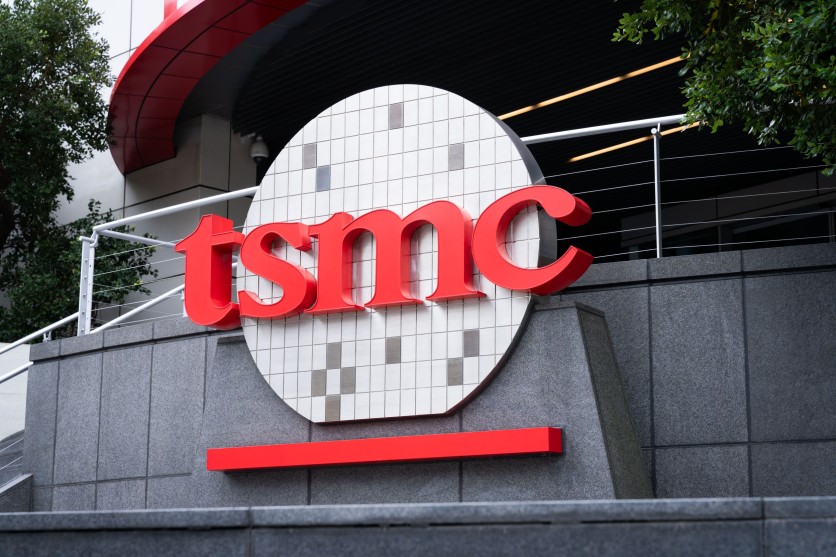
The TSMC logo is displayed at the Taiwan Semiconductor Manufacturing Company branch and Innovation Museum, highlighting the company branding and signage inside and outside the site in Hsinchu, Taiwan, January 27, 2026. Jimmy Beunardeau/Getty Images
TSMC, the world's largest chip foundry, has opened its first design center in Europe — in Munich, the heart of Germany's auto industry — as it builds out a design-to-production ecosystem on the continent and works more closely with customers from the earliest design stage. The Taiwanese company held an opening ceremony for its European Union Design Center, delivering on a plan it first unveiled at its 2025 technology symposium. The center makes Munich its 10th design center worldwide and its first in Europe, adding to a network that had spanned Taiwan, China, Japan, Canada, and the United States.
The reason a design center — not just another fab — is the news here takes a moment to unpack, and it is the whole point of the move.
Why a Design Center Is a Competitive Weapon
A fab makes chips; a design center embeds TSMC inside the customer's product before a chip is ever built. Through what the industry calls Design-Technology Co-Optimization, TSMC's engineers work alongside a customer's designers from the earliest stage, tuning the chip's design and TSMC's manufacturing process to each other to shorten development cycles and improve yields. The catch, for rivals, is that a design co-optimized for TSMC's process is expensive to move elsewhere. Engaging clients at the sketch stage does not just speed development — it quietly locks them in, which is why analysts read the European push as widening TSMC's lead over rivals on customer relationships, not only on technology.
That is also why the location matters. TSMC chose Munich for its proximity to European customers: the city is home to BMW and a short reach from Mercedes-Benz and the Volkswagen Group, and Apple already runs its largest European engineering hub there. The center is built to support European customers designing high-density, high-performance, and energy-efficient chips, with a focus on automotive, industrial, AI, and IoT applications.
Read more: TSMC Arizona Fab Posts $514M Year-One Profit: Q1 2026 Earnings Surpass Full 2025 Figure
The Memory Shift Behind Tomorrow's Car Chips
The center's technical focus points at a specific change in how car chips are built. As automotive microcontrollers move to ever-smaller manufacturing nodes, the embedded flash memory they have long relied on stops scaling well below about 16 nanometers. TSMC plans to cultivate local expertise in the replacements: non-volatile memories called RRAM and MRAM. The company has already qualified 28-nanometer resistive RAM for automotive use, with 12- and 6-nanometer versions in the pipeline, and has 22-nanometer magnetoresistive RAM in production with smaller nodes following. Those memories are what let next-generation automotive microcontrollers move beyond older embedded-flash designs — the kind of chips software-defined vehicles and driver-assistance systems increasingly demand. Beyond technical support, TSMC plans to fund doctoral research in AI and non-volatile memory with European universities and expand local hiring.
Tied to the Dresden Fab, Mirroring the Japan Playbook
The design center is closely tied to TSMC's European factory: the ESMC plant in Dresden, a roughly €10 billion joint venture with Bosch, Infineon, and NXP — the three European partners each holding a 10% stake — which is on track for volume production by the end of 2027, initially on mature 28-to-12-nanometer processes. Designs developed in Munich can flow straight to Dresden for manufacturing.
The combination mirrors a model TSMC validated in Japan, where it linked design centers in Yokohama and Osaka with its JASM fab in Kumamoto — collaborating with customers at the design stage and then handling production, widening its customer touchpoints. The push targets Europe's automotive chip market, where demand is climbing with the spread of software-defined vehicles and autonomous driving.
The Widening Lead Shows Up in the Numbers
TSMC is expanding production and R&D simultaneously across the U.S., Japan, and Europe. The company has secured additional land near its Arizona fab — enough, its leadership has said, to support roughly a decade of expansion, though it has cautioned that even that could fall short over the long run.
The lead shows up in the market data. According to Counterpoint Research, TSMC's global foundry share rose from 69% in the fourth quarter of last year to 73% in the first quarter of this year, while Samsung Electronics' share slipped from 8% to 7%. Analysts see TSMC's expansion of design support into Europe — following the U.S. and Japan — as widening the gap with rivals not just on technology but on customer relationships: by engaging clients from the initial design stage, the thinking goes, TSMC makes process optimization and faster development possible while locking in customers, leaving latecomers such as Samsung less room to break in.
Read more: Samsung Bundles Memory With Foundry Pitch to Lure MediaTek From TSMC
For Europe, the center is a step toward the local chip ecosystem the region has been trying to build. For TSMC, it is one more place where the company gets to the customer first — and the earlier it gets there, the harder it is for anyone else to follow.
Frequently Asked Questions
Why did TSMC choose Munich for its European design center?
TSMC chose Munich for its proximity to European customers. The city is home to BMW, within reach of Mercedes-Benz and the Volkswagen Group, and hosts Apple's largest European engineering hub. It also sits close to TSMC's ESMC fab in Dresden, letting the company pair design work with nearby manufacturing.
What is a chip design center?
A chip design center is a facility where a foundry like TSMC works directly with customers to develop chip designs, rather than just manufacturing finished designs. Through Design-Technology Co-Optimization, engineers tune the chip design and the manufacturing process together to improve performance and yield — and, in the process, tie the design closely to that foundry.
What is TSMC's foundry market share?
According to Counterpoint Research, TSMC's share of the global foundry market rose to about 73% in the first quarter of 2026, up from 69% the previous quarter, while Samsung Electronics slipped to around 7%. TSMC's lead rests on both its manufacturing technology and its deepening design-stage relationships with customers.
Why are RRAM and MRAM important for car chips?
As automotive microcontrollers move below about 16 nanometers, the embedded flash memory they traditionally use no longer scales well. Non-volatile memories like resistive RAM (RRAM) and magnetoresistive RAM (MRAM) are the replacements, and TSMC is developing them for automotive use — enabling the more capable chips that software-defined vehicles and driver-assistance systems require.
-
 C114 Communication Network
 -
 Communication Home
