

(Image credit: Ken Shirriff via righto.com)
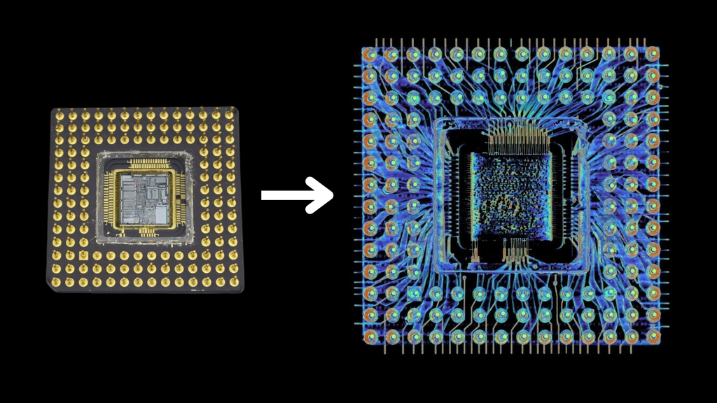
In today's world of bleeding-edge processes and packaging techniques, the Intel 386 doesn’t look like much—a grey ceramic slab with 132 gold pins, something you’d expect to find rattling around in an old parts bin at this point. But behind that dull façade lies a marvel of late-1980s chip packaging, the kind of engineering we've taken for granted. Using a CT scanner and some clever digital dissection, Ken Shirriff managed to explore every layer of this classic CPU without once touching a screwdriver or desoldering gun.
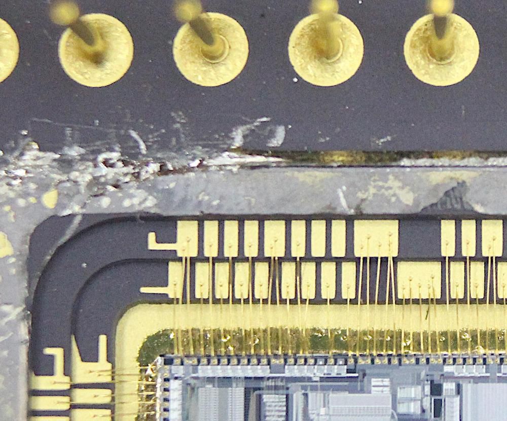
The scan produced hundreds of razor-thin X-ray slices, which were stitched into a 3D model you can spin, zoom, and digitally “peel” layer by layer. The first reveal is a halo of gold bond wires, each just 35 µm thick, far thinner than a human hair, radiating from the silicon die. These act as microscopic suspension bridges between the die’s pads and the package’s internal routing. Some carry simple data or control signals, others gang together—up to five on a pad—to handle the heavier demands of power and ground.
(Image credit: Ken Shirriff via righto.com)
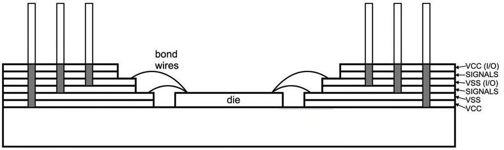
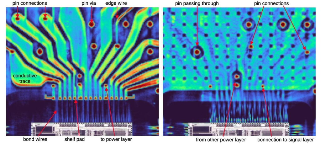
Pull back another layer, and the 386’s package shows its true sophistication: it’s essentially a six-layer circuit board in miniature. Two internal layers carry the signals while four dedicated copper planes deliver clean, stable power and ground to different sections of the chip. This “single-row double-shelf” bonding method, described in Intel’s own packaging literature attached below, was a way to cram maximum connectivity into a surprisingly compact footprint.
(Image credit: Intel via righto.com)
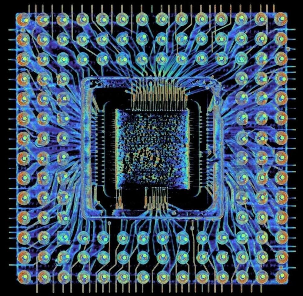
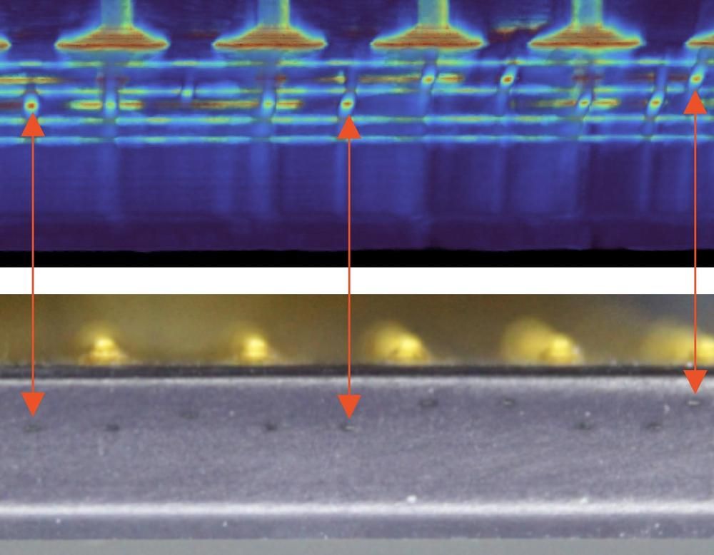
Digging deeper into the scans, Shirriff was able to map which pins connect where—some routing directly to I/O pads, others buried deep into the power and logic supply network. The CT imaging even caught details Intel probably never intended anyone to see, like the fine side wires used during manufacturing to electroplate the pins in gold. These plating contacts, barely visible spikes along the package edge, were confirmed when he lightly sanded the ceramic to match the scans.
(Image credit: Ken Shirriff via righto.com)
Moving on, the scans compare the signal and power layers side-by-side, which reveals the design’s sophistication. The signal layers are like a tangled web of thin copper paths, weaving between tiny vias, carrying all the data and control signals across the chip. They’re intricate and precise, designed to navigate the complex logic inside.
Power layers, by contrast, are almost solid sheets of copper, with only a few holes where the bond pads and vias break through. These planes deliver clean, steady power and ground to the chip, making sure everything runs smoothly without interference or noise that could cause glitches.
(Image credit: Ken Shirriff via righto.com)
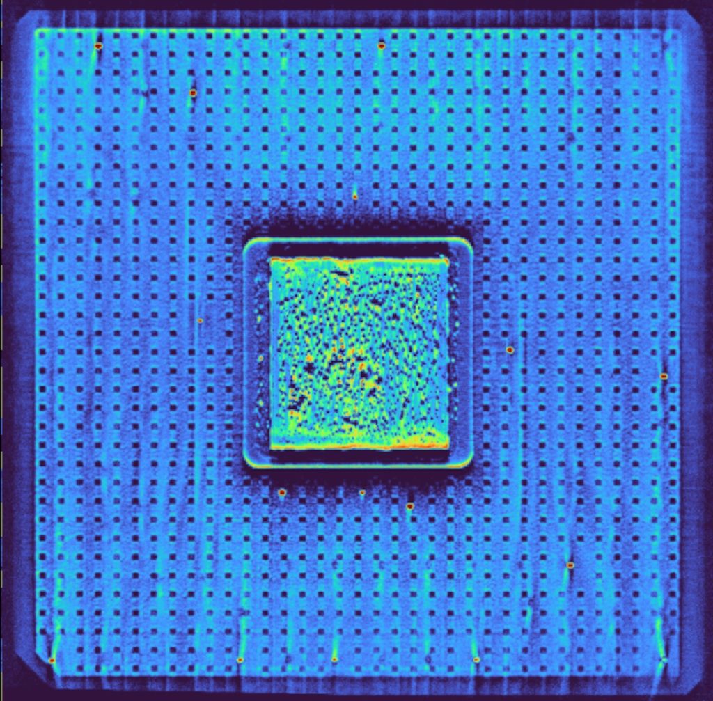
Beneath the silicon die, the X-ray reveals a bright patch—that’s silver-filled epoxy. This isn’t just glue; it’s a carefully chosen material that pulls heat away from the chip while also providing a direct, low-resistance ground connection. It’s a subtle but vital part of how the package keeps the 386 stable and reliable under load.
(Image credit: Ken Shirriff via righto.com)
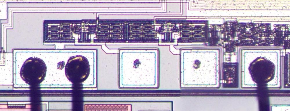
The packaging acts like a bridge across massive differences in scale. Inside the silicon die, the tiniest features are about 1 micrometer wide—barely visible even under a microscope. These then expand to wiring on the die around 6 micrometers, which connect to bond pads spaced about a quarter of a millimeter apart.
Those bond pads link to package pads spaced at half a millimeter, and finally to the pins on the bottom of the chip, spaced 2.54 millimeters apart. It’s an incredible zoom-out—roughly 2,500 times—from the microscopic core logic to the bulky socket pins you can see and touch.
(Image credit: Ken Shirriff via righto.com)
If you lined up one of the 386’s bond wires next to the socket pins it connects to, the size difference would be absurd. That’s the beauty of this packaging: it not only protects the die, but transforms it from a delicate, microscopic device into a robust, installable part you could—in theory—swap in and out of a motherboard by hand.
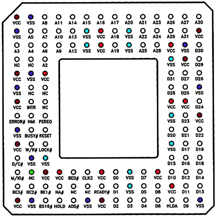
Moreover, the 386 package includes eight pins labeled as “No Connect” (NC), meaning they aren’t wired to the motherboard and appear unused. Inside the die, most of these NC pads are nearly connected, with internal wiring and pad spots ready for bond wires. Intel left these as placeholders, likely for testing or debugging during manufacturing. Interestingly, one NC pin is actually connected to the die and functions as an output, hinting at hidden signals Intel kept under wraps. Refer to the second gallery image to identify the NC pins on the die.
(Image credit: Ken Shirriff via righto.com)
(Image credit: Ken Shirriff via righto.com)
For enthusiasts, we highly urge you to check out the original blog post to learn more; it goes into far more detail for those intrigued and looking for more technicalities. For Intel, this ceramic multi-layer approach wasn’t just about elegance; it finally broke through the company's early obsession with keeping pin counts low—a relic of Intel management's 'bizarre belief that chips should never have more than 16 pins', according to Shirriff —which limited the potential of their first processors from the 70s.
The 386 marked a culmination of Intel's move to fully embrace high pin counts and advanced packaging, recognizing that complex chips demanded sophisticated, multi-layered ceramic packages to handle power, signal integrity, and heat. This shift was pivotal, enabling the performance leaps that made modern computing possible.
It’s easy to forget now, but the 386 was the CPU that made contemporary multitasking PCs possible, and its packaging was as important to that leap as its transistor count. Shirriff’s CT scan work doesn’t just satisfy curiosity; it’s a reminder that in the early microprocessor wars, Intel invested some of the world’s best engineering talent into what seemed like the most mundane aspect—"the box it comes in." Only time will tell if the once-iconic innovation powerhouse will return to its former glory.
Follow Tom's Hardware on Google News to get our up-to-date news, analysis, and reviews in your feeds. Make sure to click the Follow button.
-
 C114 Communication Network
 -
 Communication Home
