

(Image credit: Majsterkowanie i nie tylko, on YouTube)
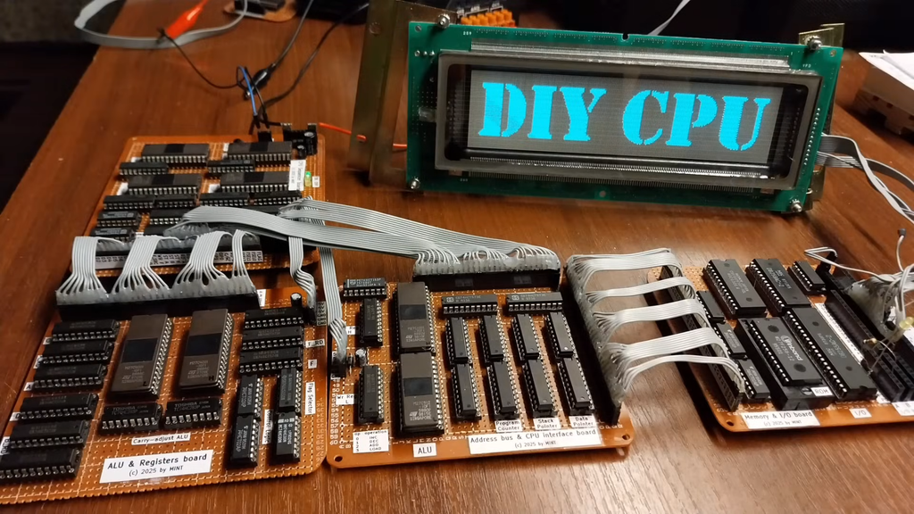
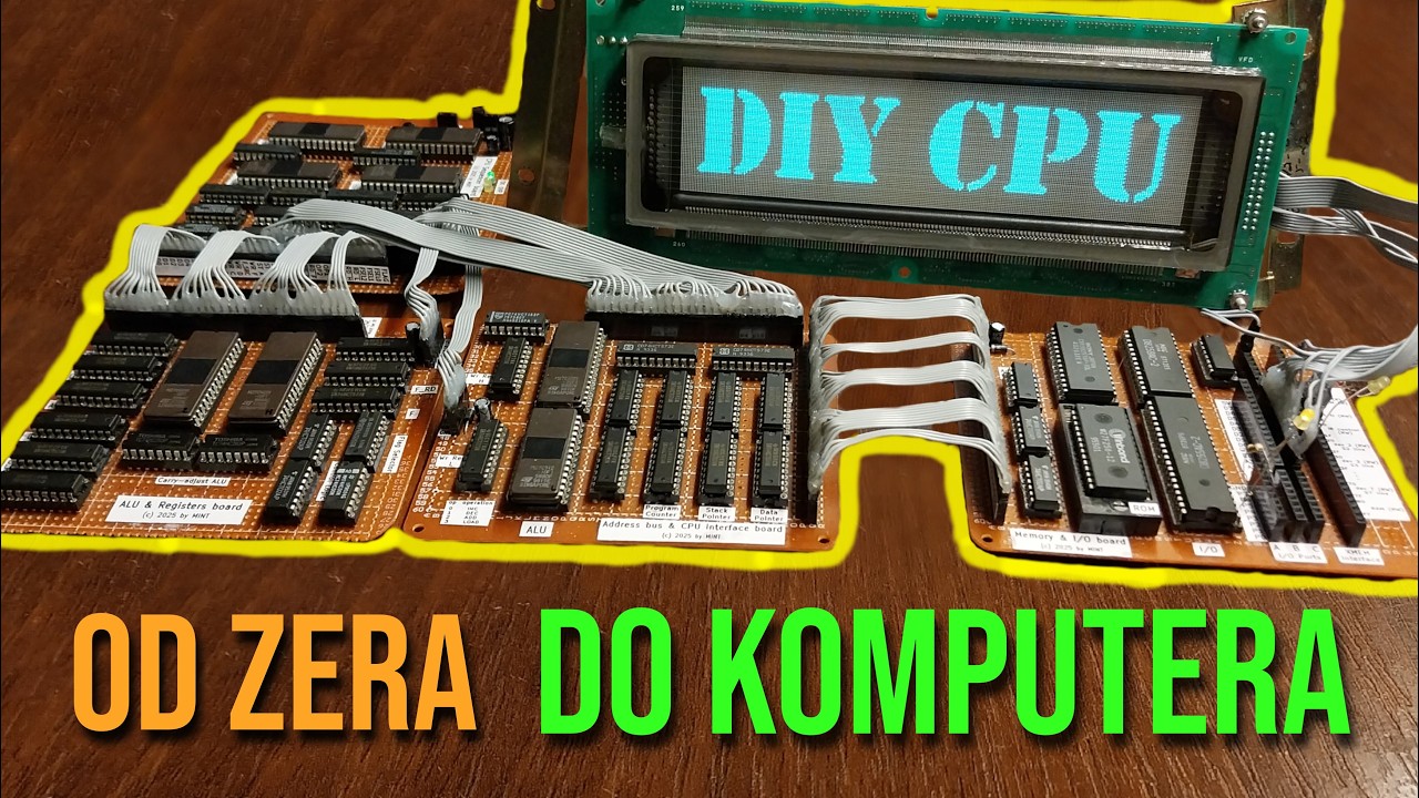
At first glance, this mess of wires, onboard components, and manually soldered circuits may seem like some sort of cyberpunk sculpture, but it's actually a project that can only be described as absurdly brilliant. A passionate enthusiast has just built an entire processor—yes, not a development board, not a microcontroller, but a full-on, instruction-capable, memory-addressing CPU using nothing but old memory chips and logic components from the 8-bit era. It wasn’t designed to replace a modern CPU, but rather a "fun" DIY project, dubbed the EPROMINT.
The creator behind this astonishing project, Majsterkowanie i nie tylko (or MINT for short, "DIY and more" in English), spent three months designing, wiring, programming, and documenting every last detail of the processor’s architecture. The idea was born from a simple experiment using obsolete memory chips called EPROMs, originally configured to control small external systems, like a PWM dimmer or a message display. The simplicity of that setup lit a spark. If memory could be used to simulate basic logic, then perhaps the building blocks of a complete processor weren’t so far off.
Not long after, the hobbyist found himself knee-deep in schematics, replicating the structure of classic CPUs from the 8-bit era, specifically those like the Z80, which helped ignite the personal computer revolution. The result is a machine that may not look sleek or polished, but functions according to real instruction sets, executes its own assembler code, and reacts to hardware interrupts just like a commercial processor would.
The project started with the most basic component of any processor: the Arithmetic Logic Unit (ALU). The first prototype, built to handle simple addition, was unreliable and had to be scrapped. Its replacement was fully socketed for easier debugging. From there, the build expanded to include a memory interface, an address bus controller—driven by a secondary ALU—and eventually the control logic, which decodes opcodes and coordinates the entire data flow.
The software was also written entirely from scratch. Nearly 2,000 lines of code were developed to define how the processor handles instructions, streamline how data moves through the system, and create testing procedures—all built using a custom set of development tools made for earlier circuit boards. The instruction set went well beyond what old-school CPUs could do, including operations like multiplication, division, trigonometric calculations, and even handling sequences of bits. As the creator put it, the processor was “dosed with steroids.”
(Image credit: Majsterkowanie i nie tylko, on YouTube)
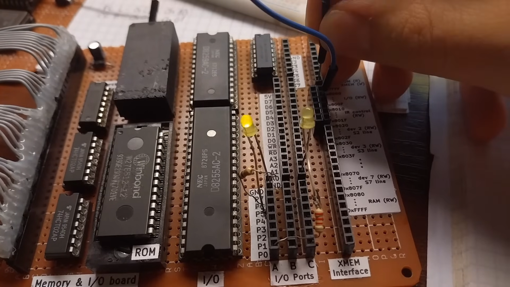
With all the modules connected, the CPU was powered on for the first time, drawing 250mA of current. The same development setup previously used for other memory chip experiments was adapted to generate a complete set of instructions for the new processor. As you can see above, a blinking LED acted as the first test program while the second LED was connected to light up when an interrupt was detected, demonstrating that the CPU could handle external events even while executing instructions. It would temporarily halt its current operation, process the interrupt, and then pick up exactly where it left off, just like a real processor.
In the end, the newly birthed CPU spanned four full-sized perfboards, weighed over 500g, and contained more than a kilometer of wire if laid out. Every logic operation was implemented using pre-programmed memory. So instead of using physical NAND gates made in silicon, the system sends an 8-bit input to an EPROM, which returns the result from a stored lookup table. Functions like data routing and instruction decoding all rely on this method. To demonstrate that the system worked, he connected it to a VFD screen and wrote code to play The Matrix... or at least, low-res fragments of it.

(Image credit: Warner Bros. / Majsterkowanie i nie tylko)

(Image credit: Warner Bros. / Majsterkowanie i nie tylko)

(Image credit: Warner Bros. / Majsterkowanie i nie tylko)
Unlike silicon buried inside a modern SoC, this processor's execution path is completely exposed. Every clock cycle, every opcode, and all register changes are visible and traceable. That’s part of the beauty. This is DIY in the truest, most punk-rock sense of the word. Watching this video makes you realize how the CPUs inside our own computers are like magic—billions of transistors dancing across the finest grains of sand, puppeteered by glass and sheer human will. If building a basic processor is this difficult, just imagine the scale of manufacturing ambition companies like TSMC have achieved. If you'd like to see similar DIY accomplishments, check out the unofficial Steam Controller 2 made from a spliced-up Steam Deck, or an RTX 5090 being brought back to life.
Follow Tom's Hardware on Google News to get our up-to-date news, analysis, and reviews in your feeds. Make sure to click the Follow button.
-
 C114 Communication Network
 -
 Communication Home
